Introduction to Integrated Photonics
If you're new to integrated photonics, knowing where to start can be a challenge. Here you can learn the fundamentals of photonic chip design and how GDSFactory tools help you put them into practice. No prior knowledge of photonics is assumed.
What is photonics?
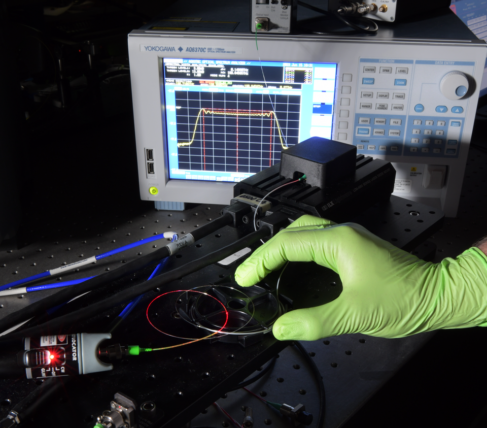
Red laser light in an optical fibre, shown for demonstration. Photo: Jennifer Lauren Lee/NIST.
Photonics is the science and technology of generating, guiding, manipulating, and detecting light. Its applications include transmitting information through optical fibres, measuring distance and chemical composition, and performing computations with optical signals. This introduction focuses on integrated photonics: designing optical components and circuits on chips.
What is a photonic integrated circuit?
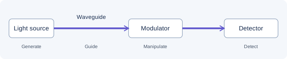
A photonic integrated circuit (PIC) combines optical components on a shared substrate to perform functions such as generating, guiding, manipulating, and detecting light. Which functions can be integrated on the chip depends on the materials and fabrication process; for example, the light source may be on the chip or (more commonly) coupled in from an outside laser.
Photonic circuits directly use light to process data. Integrated circuit component geometry and optical path length affect the behaviour of electromagnetic fields and remain the subject of an immense amount of research. Networks of these components can implement filters and other signal-processing operations in a compact footprint, especially as compared to bench-top optical test setups. Precise fabrication helps reproduce the intended geometry and is what makes photonic integrated circuits uniquely scalable and capable in the technological landscape.
How are photonic circuits designed and simulated?
Designing a photonic circuit involves modelling individual devices, connecting and arranging them on a chip, and checking the resulting photonic circuit's behaviour and layout. A wide variety of tools can be used for each of these steps, but packages associated with the broader GDSFactory project will be emphasized for their interoperability and open-core philosophy.
Device simulation
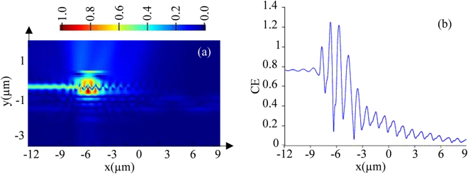
Example grating coupler FDTD simulation. Figure 3 from Asaduzzaman et al., Scientific Reports (2018), reproduced unchanged under CC BY 4.0.
Device simulation predicts electromagnetic behaviour from geometry and material properties. Devices that are commonly simulated include:
- Waveguides: structures that confine and guide light between components; common types include slab and rib waveguides.
- Waveguide bends: curved sections that change the direction of guided light and induce heavy loss if not designed carefully.
- Directional couplers: closely spaced waveguides that transfer light between them through overlapping optical fields.
- Grating couplers: periodic structures that diffract light between an on-chip waveguide and an external beam, typically from an optical fibre.
- Mach–Zehnder interferometers (MZIs): structures that split light between two arms and recombine it so the relative phase controls the output power; electrically controlled phase shifters enable operation as modulators.
- Ring resonators: closed-loop waveguides coupled to adjacent waveguides that selectively resonate at particular wavelengths; electrically shifting the resonance enables operation as modulators.
Simulations help quantify transmission, reflection, and loss in these devices. For an example of comparing a device model with measurements, Ballesteros, Matres, Martí, and Oton (2011) show how backscattering changes a silicon ring resonator's spectral response.
You can use packages such as gSim and MEOW for simulation techniques including finite-difference time-domain (FDTD), finite-element methods (FEM), and eigenmode expansion (EME). FDTD evolves fields on a spatial grid; FEM approximates fields over a mesh; EME represents propagation through successive sections using their supported modes. Each method has trade-offs; arguably the most important of these techniques, FDTD, offers flexibility across device geometries but can require substantial computing time and memory.
Component layout
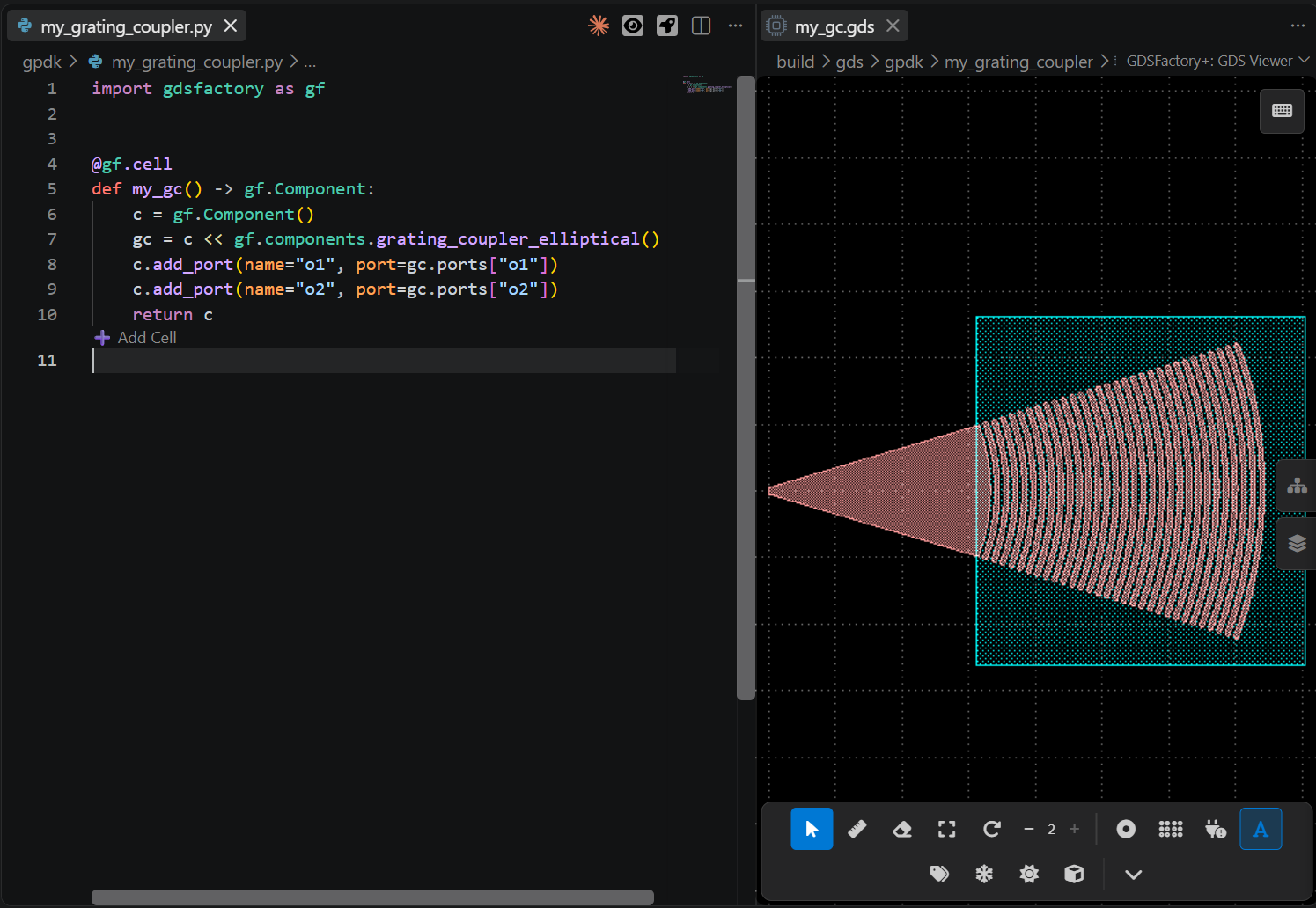
GDSFactory+ Advanced Workflow: Layout Aware Design — Creating a custom component and inspecting it in the GDS Viewer. In this example, my_gc() is our custom component, and it's being populated by a subcomponent provided by the gdsfactory generic PDK.
Component layout translates an individually simulated device design (originally conceived as 3D geometry) into shapes on fabrication layers. Foundry process knowledge determines the available materials, layer thicknesses, minimum feature sizes, and manufacturing tolerances. With the open-source gdsfactory Python library, you can define reusable, parameterized Components, their Ports, and how subcomponents are handled, such as with waveguide bundles. A component's layout specifies only that device's geometry and forms the basis of PDK libraries. Larger photonic circuits can be laid out all at once using only the open-source gdsfactory library, but that makes it more difficult to perform system-level analysis and circuit simulation.
GDSFactory: An Open-Source Python Library for Chip Design and Simulation, coauthored by GDSFactory company leadership, describes parameterized layout and its connections to simulation and verification.
Circuit design
Photonic circuit schematics
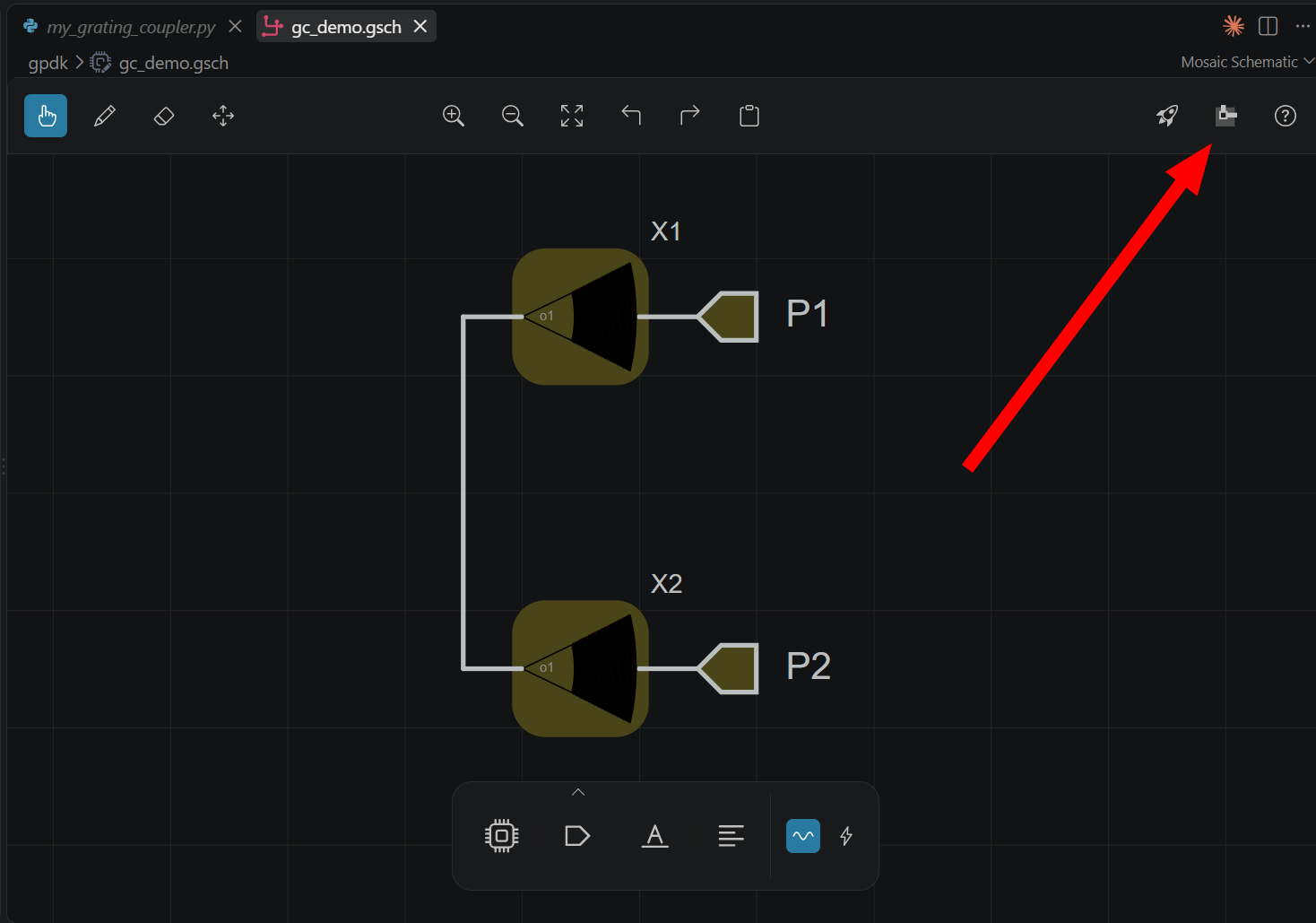
GDSFactory+ Advanced Workflow: Layout Aware Design — Two instances of the custom my_gc() component are placed in a schematic and their ports are connected. The red arrow indicates that there is a parallel layout view of this same schematic, as seen in the next section.
A larger photonic circuit with multiple components can be represented as a block-diagram schematic, which can help with abstracting a circuit's intended operation, such as ensuring an ideal modulator reaches a certain requisite bandwidth. However, a block diagram can't represent physical relationships between components, the same way an electrical circuit diagram with resistors and capacitors can't represent how far the components will be placed from one another. A photonics circuit designer must always keep in mind how the layout will affect their chip's performance, both in footprint and how the physics will affect the optical signals.
Photonic circuit layout
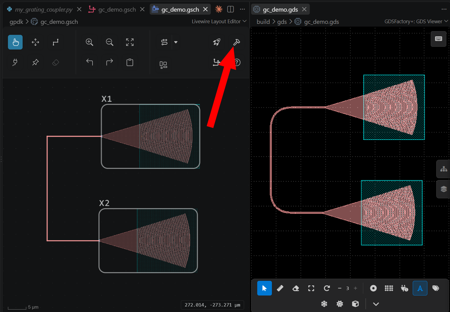
GDSFactory+ Advanced Workflow: Layout Aware Design — The schematic is translated into a layout before generating the geometry as a viewable .gds file.
Circuit layout is similar to component layout, but bigger. Placement and routing must preserve the schematic's connectivity while fitting within the die and meeting requirements for spacing, bend radii, and optical and electrical access. These physical choices also affect circuit behaviour: moving a component can lengthen a connecting waveguide, changing its propagation phase and loss even though the block-diagram connection is unchanged. Design for manufacturability (DFM) extends this consideration to fabrication tolerances, so the design accounts for how the manufactured geometry may vary. Connectivity, placement, and routing therefore need to be considered together.
The GDSFactory+ Schematic Editor and Layout Editor are examples of tools that provide linked graphical views of this design, letting you define connections, position components, and route them before evaluating the circuit's response through simulation.
Circuit simulation
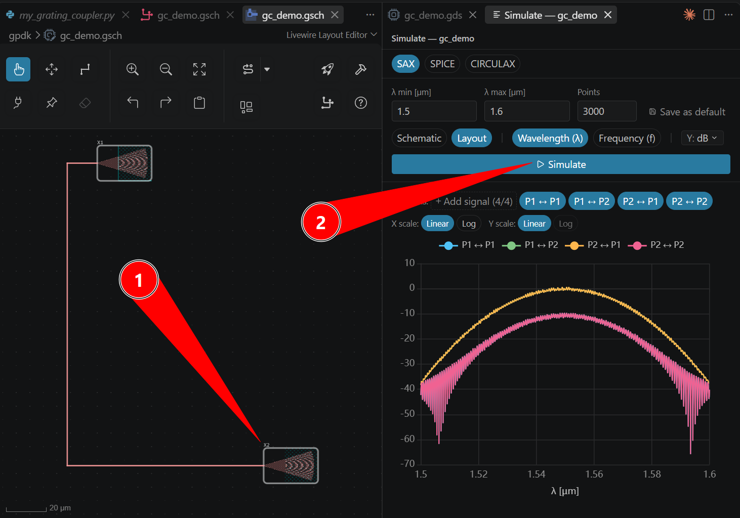
GDSFactory+ Advanced Workflow: Layout Aware Design — Increasing the routed path length between couplers changes the simulated resonance spacing.
Circuit simulation combines component models to predict the response of the connected system. SAX uses scattering-parameter models for frequency-domain analysis, such as calculating transmission across a wavelength range. Circulax supports time-domain analysis, such as following a circuit's response to a changing input, as well as steady-state analyses. Model parameters must represent the intended devices and interconnections, including routed lengths when predicting layout-dependent behaviour.
Physical layout inspection
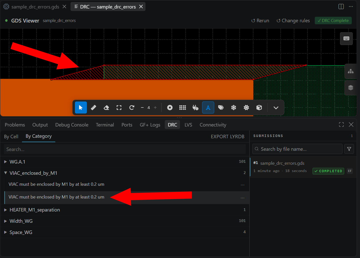
GDSFactory+ DRC Quickstart — Selecting a reported violation highlights the affected geometry in the sample layout, helping you locate design rule errors before fabrication. Pictured is GDSFactory+'s built-in GDS viewer, powered by KLayout.
KLayout lets you inspect the geometry in a GDS layout and run verification scripts. Design rule checking (DRC) tests geometry against rules such as minimum widths and spacing. Layout versus schematic (LVS) compares connectivity extracted from the layout with the intended circuit. Both require rules and extraction definitions appropriate to the fabrication process; visual inspection alone does not establish either result.
How does a design become a chip?
With your design complete and verified, you're ready to send it to be fabricated into a physical chip.
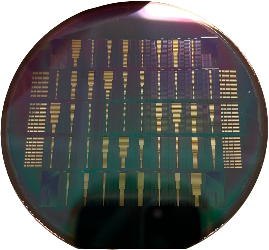
Photonic chips fabricated on a silicon wafer. Photo: N. Nader/NIST.
Throughout the design process, your chip must be designed for the material stack and fabrication process offered by a foundry. In fact, these foundry guidelines take up a lot of a photonic chip designer's headspace, as each fab process has its own quirks that impact a circuit's operation in unexpected ways. The foundry's process design kit (PDK) provides layer definitions and design rules, and may include component libraries and simulation models, which can help bridge the gap between designer and wafer. One example of a frontier in fab processes and chip design is silicon photonics; GDSFactory tools support it and other material platforms through platform-specific PDKs. For more information, Khan and colleagues' review, Photonic Integrated Circuit Design in a Foundry+Fabless Ecosystem, explains how PDKs connect circuit designers to foundry processes and how fabrication variability and packaging requirements influence design, with an emphasis on silicon photonics.
Where does GDSFactory+ fit?

GDSFactory+ connects Python component design, graphical schematics, placement and routing, circuit simulation, and GDS inspection in one design environment. Its schematic and layout editors share a circuit description, helping you evaluate how physical design choices affect circuit behaviour. The open-source packages remain independently usable; GF+ adds integrated workflows, consistent with the project's open-source philosophy.
To get started with the GDSFactory+ workflow, start by making a cell in Create a Cell, or to try the graphical workflow, continue to Design Your First Circuit.
Further reading
- Bahaa E. A. Saleh and Malvin Carl Teich, Fundamentals of Photonics. A textbook covering wave optics, waveguides, light sources, modulation, and detection across material platforms.
- Lukas Chrostowski and Michael Hochberg, Silicon Photonics Design. A practical reference for devices, fabrication, layout, and circuit modelling; Chapter 9 covers photonic circuit modelling.
- José Capmany and Daniel Pérez, Programmable Integrated Photonics. Photonic building blocks, network theory, and programmable circuit design.
- Daniel Pérez, Ivana Gasulla, and José Capmany, “Reconfigurable integrated waveguide meshes for photonic signal processing and emerging applications”. A review of circuit architectures and their signal-processing functions, with examples in silicon and silicon nitride.
- Muhammad Umar Khan, Yufei Xing, Yinghao Ye, and Wim Bogaerts, “Photonic Integrated Circuit Design in a Foundry+Fabless Ecosystem” (2019). A review of the relationship between circuit design, PDKs, and foundry fabrication, including manufacturing variability and packaging requirements, with an emphasis on silicon photonics.
- Ankita Sharma et al., “AI agents for photonic integrated circuit design automation” (2025). Coauthored by GDSFactory employees Vahid Ansari and Joaquin Matres, this research paper presents PhIDO, a proof-of-concept system that converts natural-language circuit descriptions into layout files.
- Wim Bogaerts and Lukas Chrostowski, “Silicon Photonics Circuit Design: Methods, Tools and Challenges” (2018). A review of schematic capture, circuit simulation, layout, and verification, including the effects of fabrication variability.
- Meint Smit et al., “An introduction to InP-based generic integration technology” (2014). A review of indium phosphide building blocks, design tools, and shared foundry processes for photonic chips.