Writing and reading PCB Gerber layouts
GDSFactory can export the copper and mechanical geometry in a Component as Gerber X2. This notebook creates a small two-layer RF test coupon, writes a Gerber fabrication package, and reads the generated top-copper image back with Gerbonara.
Units: GDSFactory coordinates are micrometres (
um), while Gerber files normally use millimetres or inches.to_gerberdefaults touminput andmmGerber output. Setlayout_unit="mm"only when the component coordinates are already in millimetres.
GDSFactory provides a Gerber writer, not a native Gerber importer. Gerbonara is used here as an optional independent parser for automated checks; use a PCB CAM viewer such as KiCad Gerber Viewer to inspect the full layer set before fabrication.
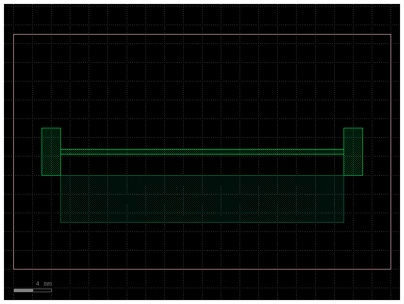
Create a board component
The generic PDK's metal layers stand in for the two PCB copper layers. They are mapped to PCB stackup names when the Gerber files are written.
from pathlib import Path

import gdsfactory as gf
from gdsfactory.gpdk import LAYER

gf.gpdk.PDK.activate()

board = gf.Component("rf_test_coupon")

# Coordinates are in um: this outline is 40 mm by 25 mm.
board.add_polygon(
    [(0, 0), (40_000, 0), (40_000, 25_000), (0, 25_000)],
    layer=LAYER.FLOORPLAN,
)

# Top copper: a 0.5 mm-wide trace and two pads.
board.add_polygon(
    [(5_000, 12_250), (35_000, 12_250), (35_000, 12_750), (5_000, 12_750)],
    layer=LAYER.M1,
)
for x in (3_000, 35_000):
    board.add_polygon(
        [(x, 10_000), (x + 2_000, 10_000), (x + 2_000, 15_000), (x, 15_000)],
        layer=LAYER.M1,
    )

# Bottom copper: a small ground plane beneath the trace.
board.add_polygon(
    [(5_000, 5_000), (35_000, 5_000), (35_000, 10_000), (5_000, 10_000)],
    layer=LAYER.M2,
)

board.plot()
Write the Gerber package
Map each GDSFactory layer to a filename and Gerber X2 file function. The file function lets CAM software identify the layer role without relying only on its filename.
from gdsfactory.export import BoardOptions, GerberLayer, GerberOptions, to_gerber

gerber_dir = Path("build/rf_test_coupon_gerbers")

written = to_gerber(
    component=board,
    dirpath=gerber_dir,
    layermap_to_gerber_layer={
        LAYER.M1: GerberLayer(
            name="F_Cu",
            function=["Copper", "L1", "Top"],
            polarity="Positive",
        ),
        LAYER.M2: GerberLayer(
            name="B_Cu",
            function=["Copper", "L2", "Bot"],
            polarity="Positive",
        ),
        LAYER.FLOORPLAN: GerberLayer(
            name="Edge_Cuts",
            function=["Profile", "NP"],
            polarity="Positive",
        ),
    },
    options=GerberOptions(mode="mm", layout_unit="um", resolution=1e-6),
    board=BoardOptions(n_layers=2),
)

print(*written, sep="\n")
build/rf_test_coupon_gerbers/F_Cu.gbr
build/rf_test_coupon_gerbers/B_Cu.gbr
build/rf_test_coupon_gerbers/Edge_Cuts.gbr
build/rf_test_coupon_gerbers/rf_test_coupon.gbrjob
Read and validate a Gerber image
Install the optional parser once with uv add --group dev gerbonara or pip install gerbonara. A Gerber package has one image per layer, so open each .gbr image separately. Here the parser confirms that the 3,000–37,000 um top-copper extents became 3–37 mm.
try:
    from gerbonara import GerberFile
except ImportError:
    print("Install Gerbonara with `pip install gerbonara` to run this check.")
else:
    top_copper = GerberFile.open(gerber_dir / "F_Cu.gbr")
    bbox = top_copper.bounding_box(unit="mm")

    assert bbox == ((3.0, 10.0), (37.0, 15.0))
    bbox
Install Gerbonara with `pip install gerbonara` to run this check.
Inspect the fabrication package
The export directory contains F_Cu.gbr, B_Cu.gbr, Edge_Cuts.gbr, and rf_test_coupon.gbrjob. The .gbrjob file records the board size, copper-layer count, and image functions. Keep it with the Gerber images and preserve their names.
For a visual check, open all .gbr files together in KiCad Gerber Viewer, then verify the outline, layer order, clearances, and dimensions. If the board is 1,000 times too large or too small, check GerberOptions.layout_unit.
The exporter writes filled polygons as Gerber regions. It does not create drill (
.drl), solder-mask, paste, or PCB-netlist files; add those manufacturing deliverables through the appropriate PCB/CAM workflow.