Advanced Workflow: Layout Aware Design with Grating Couplers
In this demo, we'll see how GDSFactory+'s schematic-driven layout workflow allows you to make design decisions while taking into account things like routing path-length and formation of backreflection cavities.
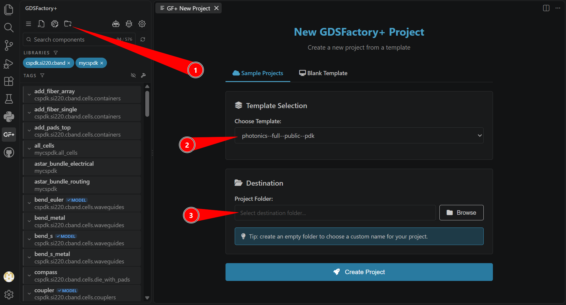
This tutorial uses the photonics-full PDK, a public resource bundled with GDSFactory+. To take full advantage of this tutorial, create a new template project with the New GDSFactory+ Project button at the top of the GF+ sidebar, select photonics--full-public--pdk from the list, and customize the destination folder. Then, use 🚀 Create Project to get started!
Review: The GDSFactory+ Graphical Workflow
Recall GDSFactory+ has three ways of visualizing your photonic circuits.
- Schematic Editor allows you to create block diagrams with ideal electrical and optical connections between Component models, without regard to the actual size of the die
- Layout & Routing Editor is a graphical way of laying out your circuit by clicking and dragging Components and routes
- GDS Viewer allows you to preview a built .gds file before sending it to a foundry for fabrication
Under the hood, all the information associated with a circuit's Schematic Editor and Layout & Routing Editor representations are contained in a single .gsch schematic file, which is stored as YAML-style plain text. This means your block diagram and layout are fundamentally connected, and is what makes GDSFactory+ 2.0 so powerful.
This demo will take full advantage of this .gsch interconnection in conjuction with the SAX simulator.
Individual components, however, are usually created with custom .py files as described by the open source GDSFactory core. By the end of this tutorial you should have a better understanding of how these environments interrelate in GDSFactory+ v2.
Create a custom grating coupler component using the python interface
Let's first create a custom grating coupler component, so we can practice combining the code and schematic environments of GDSFactory+.
-
In the top section of the app, click the button that has a file icon with a 'py' sign on it. Then type
my_grating_couplerfor the name and pressenter. This will create a Python file namedmy_grating_coupler.py, and open itsCode Viewin a new tab.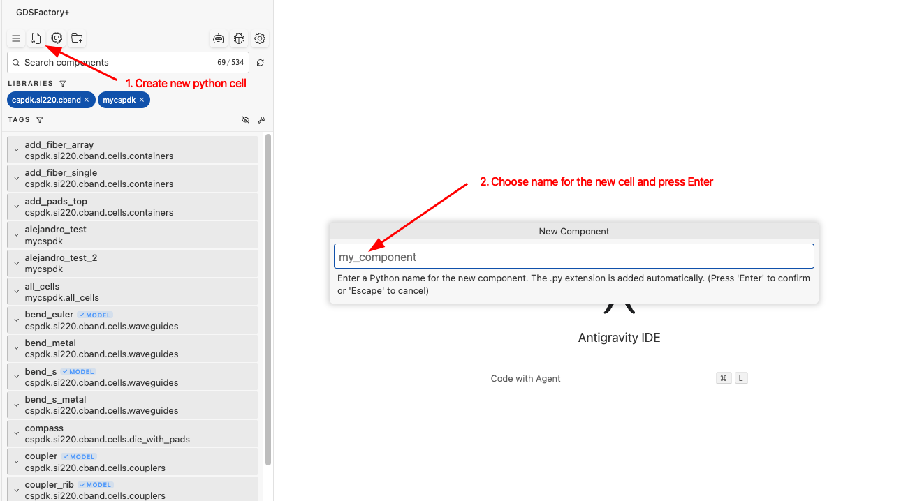
-
Replace the starter code imports with the following code:
-
In the right top bar, click the eye button. Then click
Show GDSto open theGDS Viewand verify the single grating coupler renders correctly.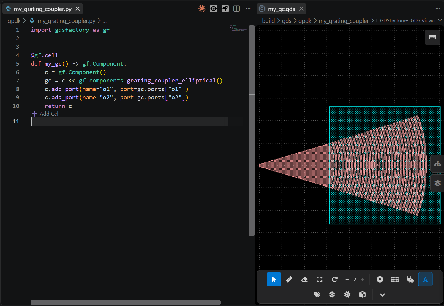
-
Now in order to simulate our custom grating coupler, we need to associate it with a SAX simulation template. On the left bar, search for your "my_gc" component and either right click or use the 3 dots right of the hammer icon to select the
⊕ Add Modeloption.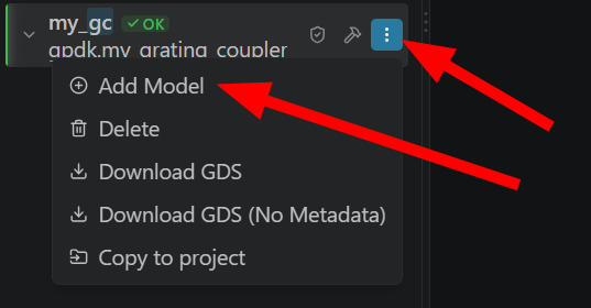
-
You can use all default options in the "Add Model" SAX window, go ahead and select
grating_couplerunder "SAX MODEL" to use the built in model. Click "Create SAX Model" at the bottom right when you're done.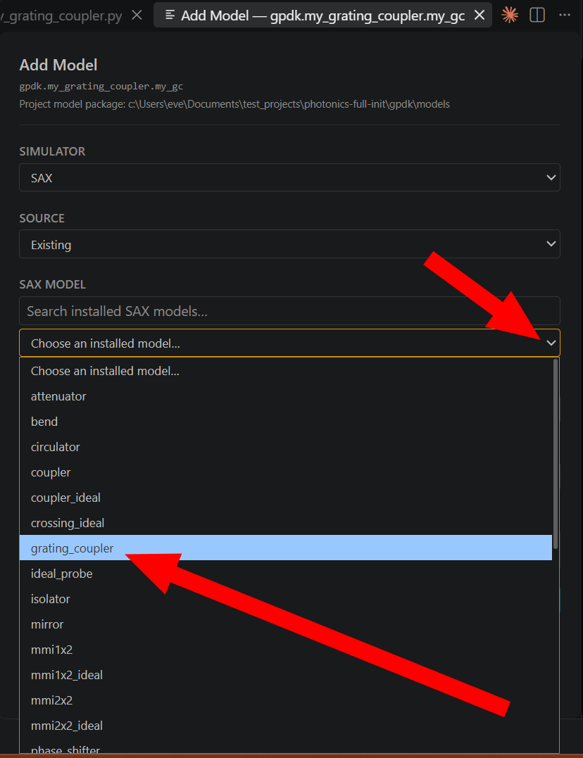
-
The SAX model definition should have opened in a new tab, in a file called
my_gc_sax.py. Let's update the defaultreflection(waveguide-side) andreflection_fiber(grating-side) values to 0.3 and 0.01, respectively.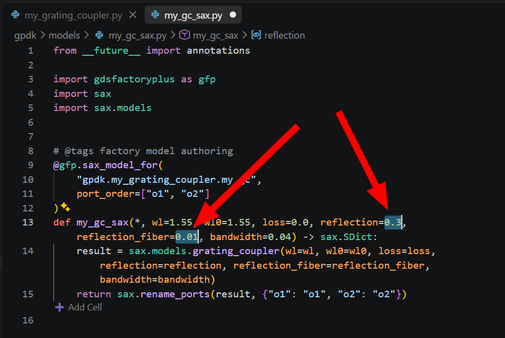
Your custom grating coupler is now ready to be added to a larger photonic circuit!
Create a schematic file
Now that you have created your own grating coupler component, let's add it to a schematic to simulate its optical behavior with relation to real layout path lengths.
-
In the GF+ tab, select the
New Schematic (.gsch)button.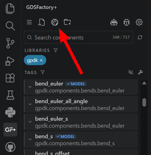
-
Above "Schematic filename" type the name of your new schematic (
gc_demofor example) and press enter to confirm. This will create a new schematic file namedgc_demoand open itsSchematic Viewin a new tab.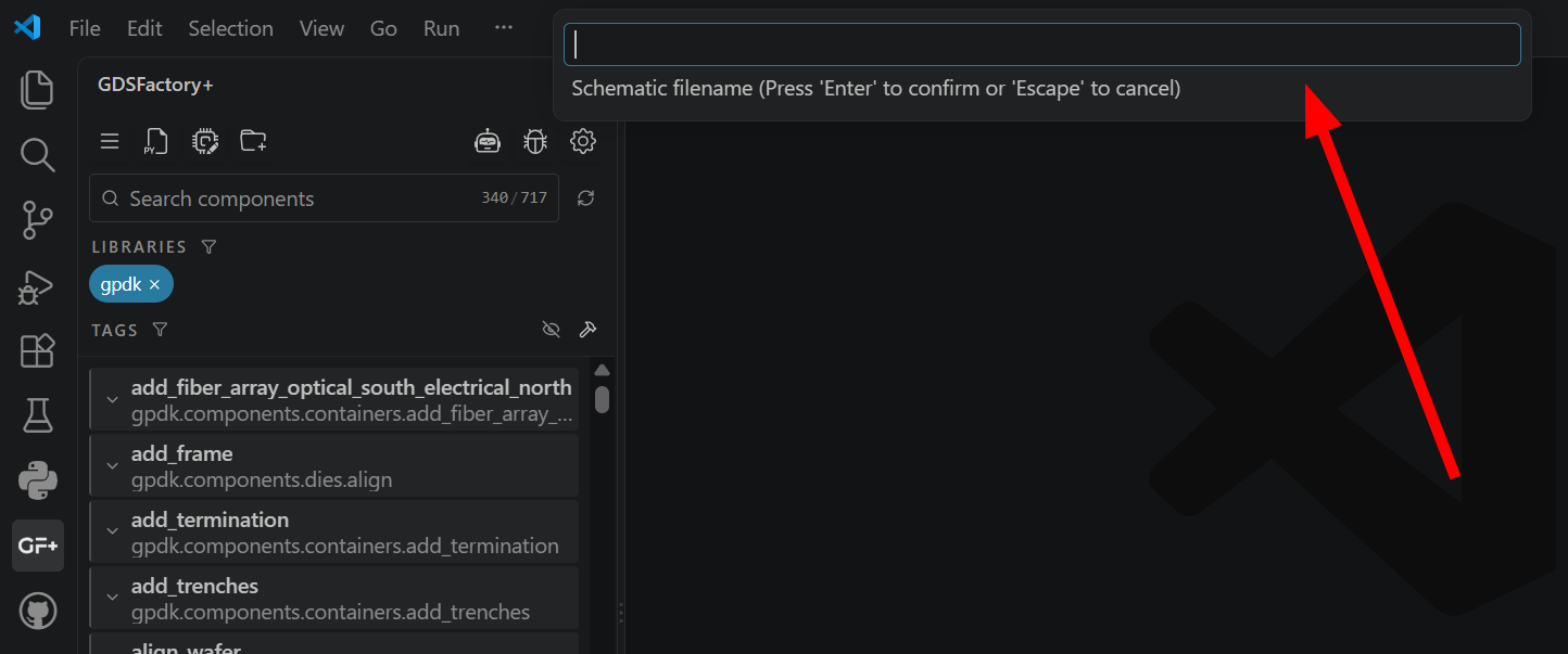
-
We'll add the couplers with the "Add component from library" button at the bottom. Select the component icon, type in "my_gc", then select
my_gcfrom the right menu. Then simply place the component twice.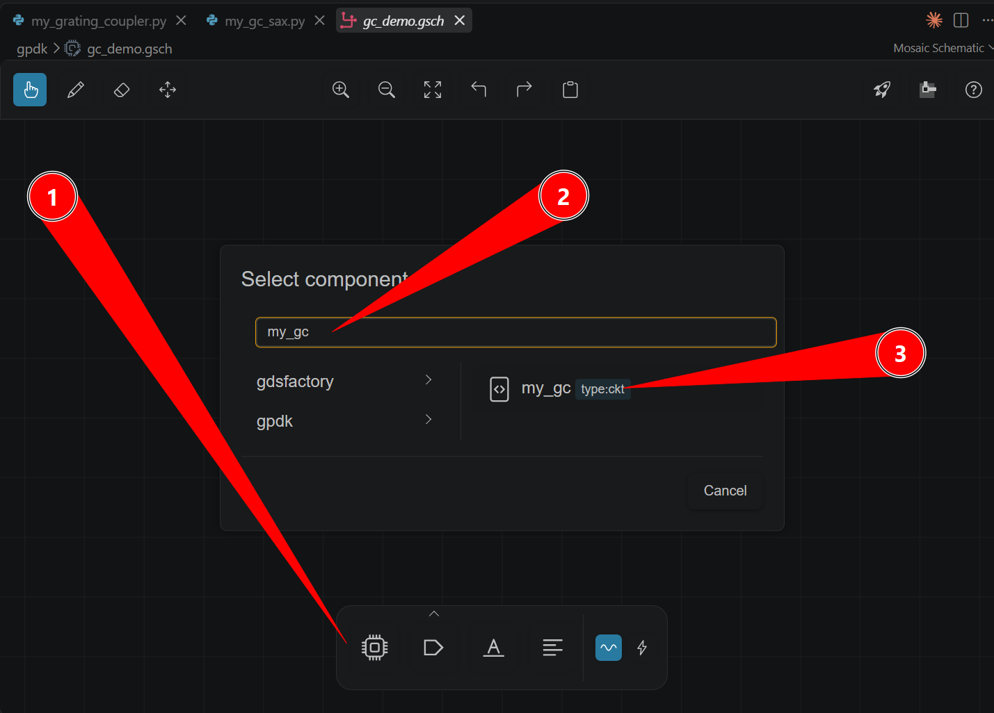
In this example, arrange the components vertically for convenience later.
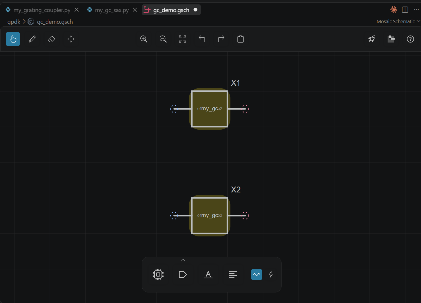
For now, don't worry if the schematic symbol doesn't immediately propagate to display a grating coupler image. Just remember that o1 on the left refers to the waveguide connection port (blue outline circle) and o2 on the right is the grating's exterior connection (pink outline circle). You'll be able to verify this later when the layout is rendered.
-
Use the "Wire" tool on the top left to connect the
o1port of both grating couplers, or just hover over the exposed o1 port of the top component and click to drag an optical connection to the o1 port of the bottom component. This may be when you see the schematic symbols update.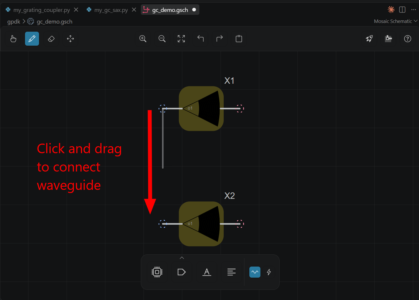
-
Use the "Add Port" tool at the bottom and click on the
o2port of both grating couplers to interface with the circuit and see its behavior later. Use the[R]key to rotate the port before you place it.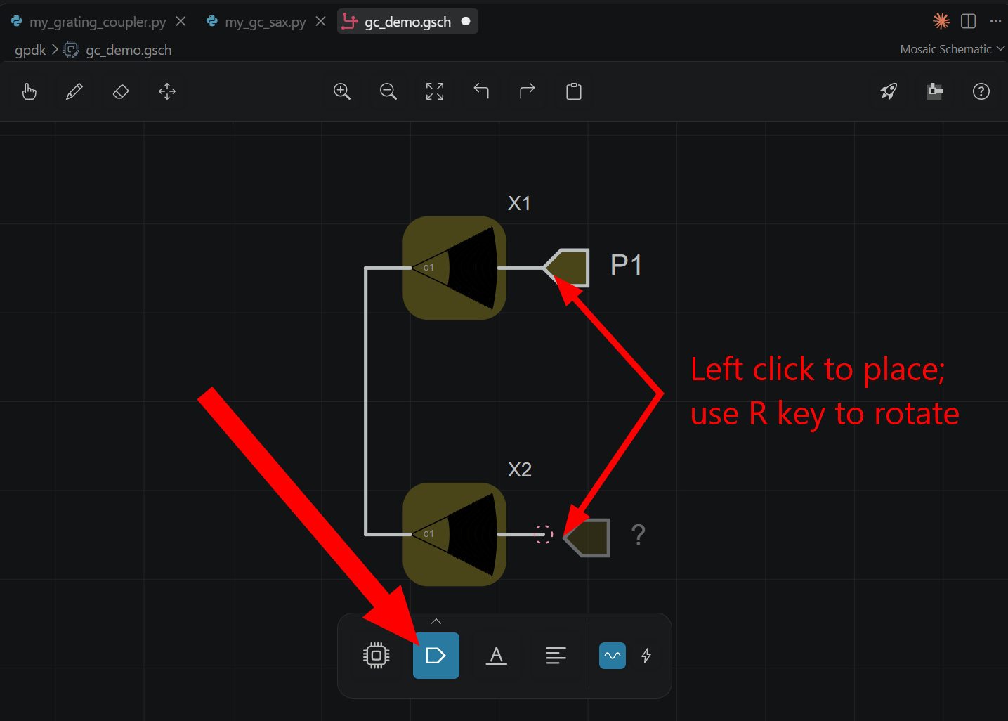
Layout: Route optical waveguide connection
Now it's time to lay out your photonic circuit. Select "Open in layout editor" on the top right.
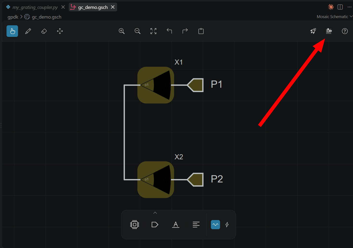
-
You should see your two grating couplers connected with a ghost wire.
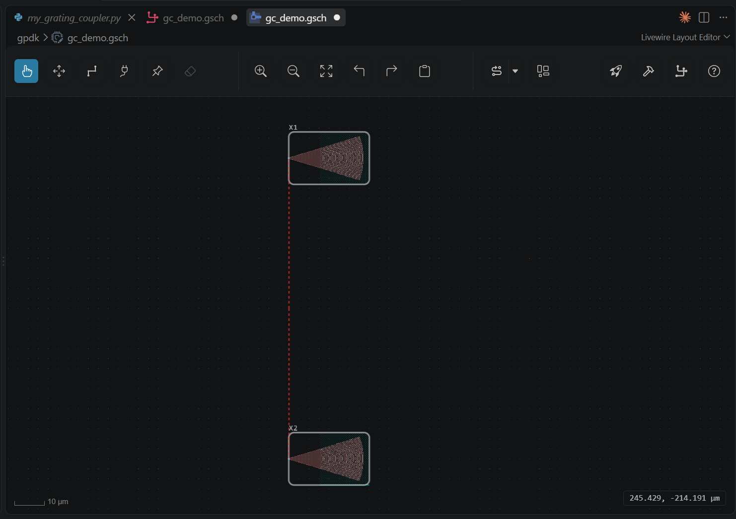
-
You have two options for routing: either manually click and drag between the appropriate ports with the Route tool in the top left (exactly the same as with the Wire tool earlier!), or let GF+ auto-route by right clicking the ghost wire or selecting "Auto Route" in the top right.
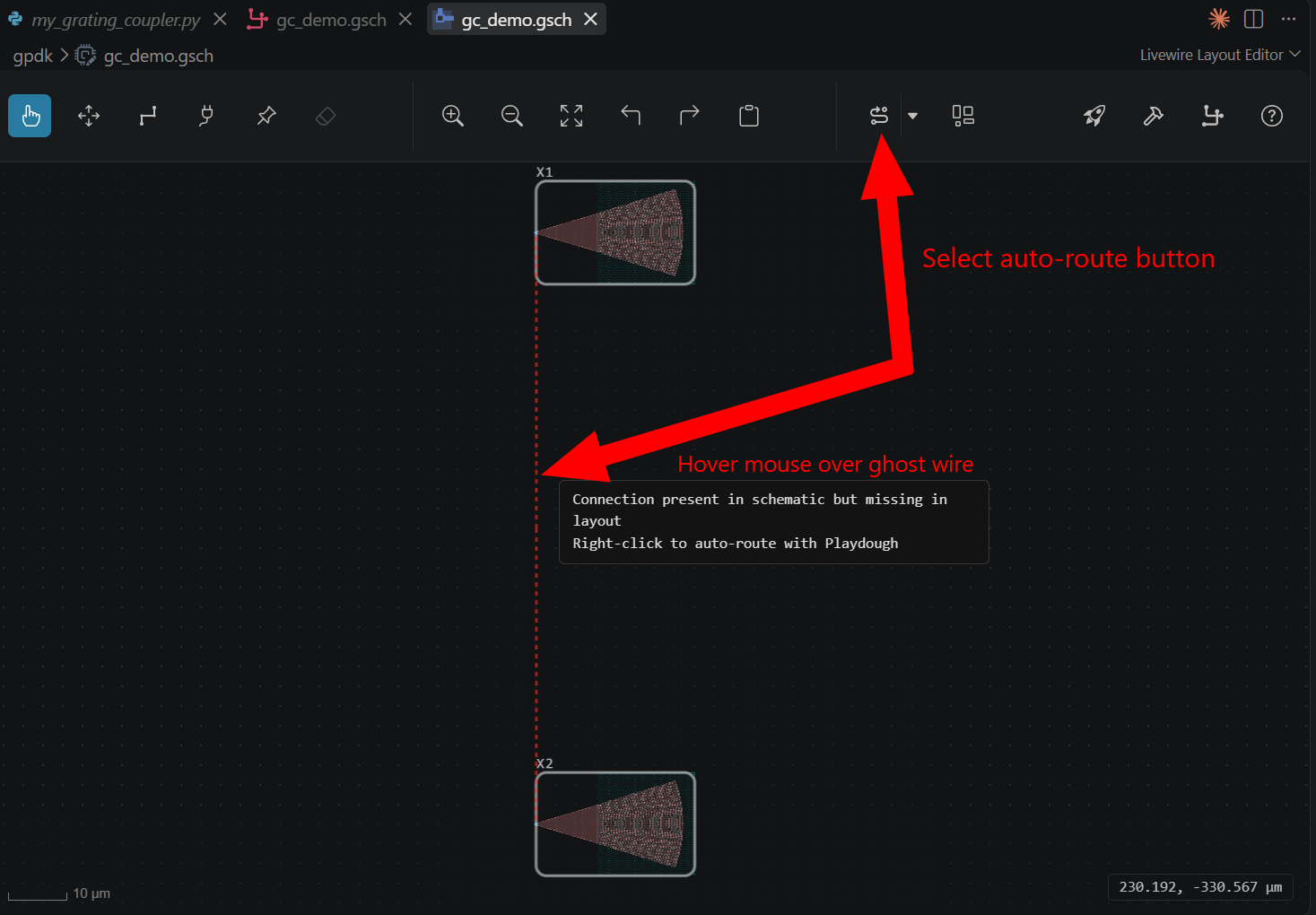
If you run into any issues with the auto-router, try toggling "Finetune" in the auto route dropdown menu > Route settings.
-
Now you can build your layout's GDS and view it with the built in GDS viewer; just select the hammer icon on the top right of the Layout Editor and the GDS should pop up in a new window.
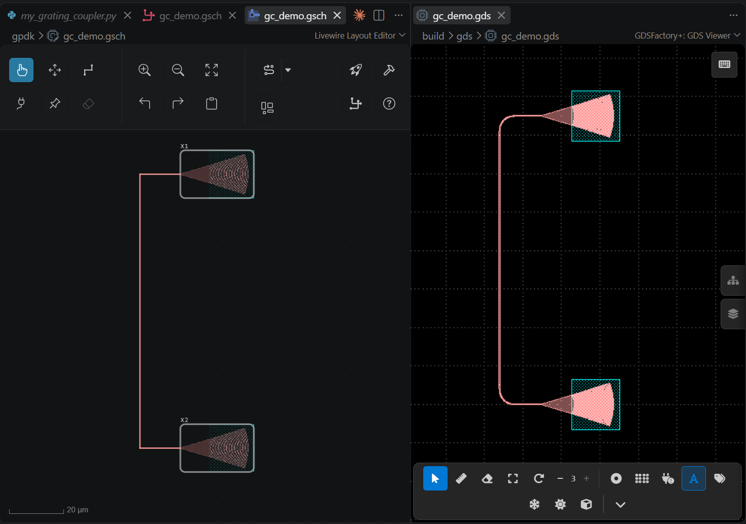
Simulate the Fabry-Perot cavity between couplers
In order to illustrate the backreflections forming a resonant cavity within your waveguide, let's run a simple wavelength sweep simulation on the two grating couplers.
-
First, practice adjusting your layout interactively by clicking and dragging the bottom grating coupler closer to the top grating coupler. This will make a short reflective cavity. Second, select the
🚀 Simulatebutton on the top right. Third, ensure theLayoutoption is selected, so SAX draws from your layout's real path length. Then hit▷ Simulate!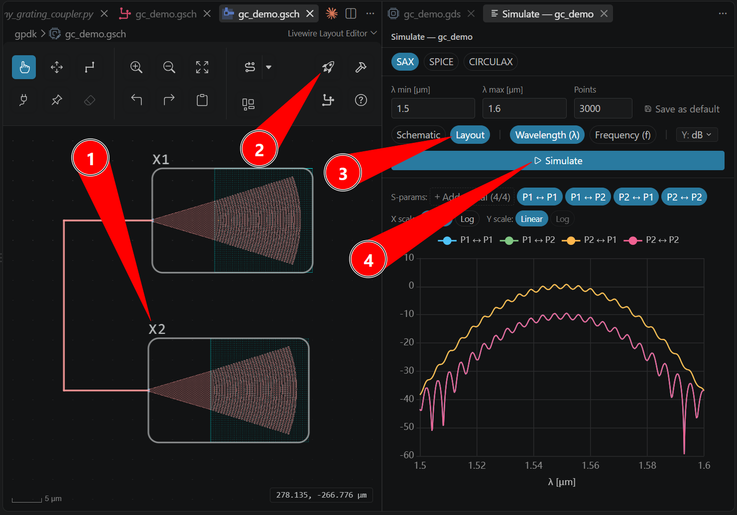
You should see a resonance forming on both the through signal (top trace) and the fiber-facing reflected signal (bottom trace) due to the high reflection values we manually added to the custom SAX model earlier.
-
Now, move the grating coupler further away in the Layout Editor, and re-run the simulation. Your
gc_demo.schshould auto-save and provide the updated layout information to SAX, which will show a much larger cavity size, meaning there are quite a few more wavelengths that are compatible with a standing-wave. This is the same mechanism that makes smaller ring resonators have larger FSR, and holds true for any resonating structure.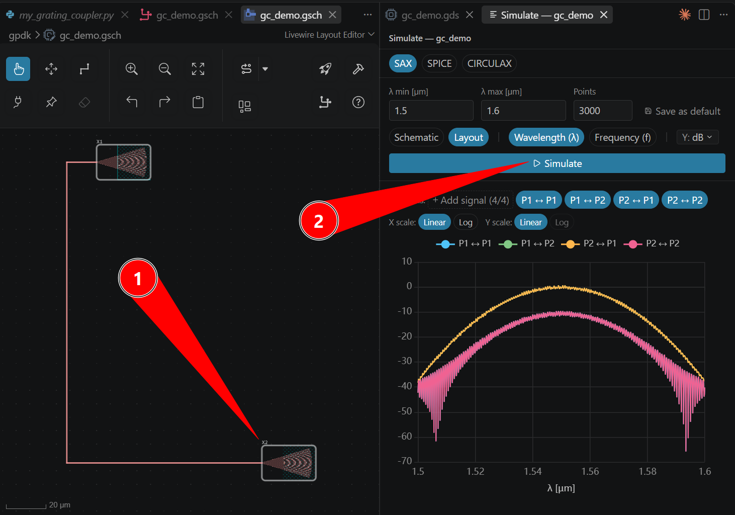
Conclusion
Congratulations! In this tutorial, you designed, laid out, and simulated a custom grating-coupler layout, and GDSFactory+ helped you identify the presence of a Fabry-Perot cavity forming between the ends of your integrated waveguide.
Extra: note about .gds file update
Note that the .gds viewer does not automatically update when you adjust the Layout Editor. To view the actual .gds layout the simulator is drawing from, simply re-select the hammer icon to Generate GDS and view the new layout with bends and placement already accounted for.
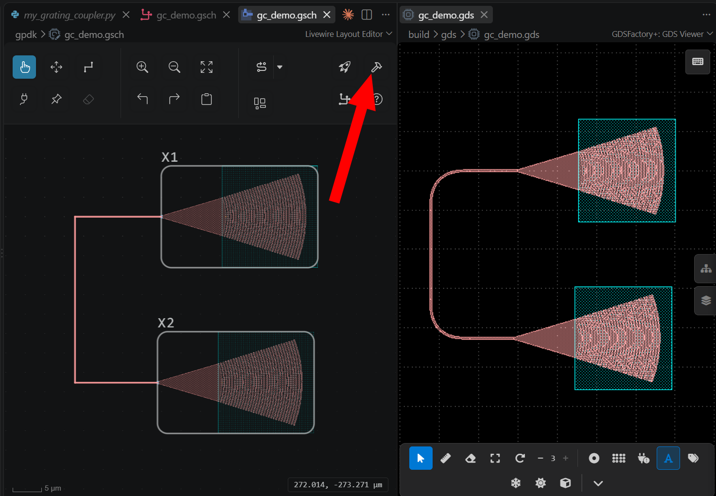
A common issue when performing layout-based SAX simulation is that the generated .gds has a problem not immediately represented within the Layout Editor, due to the abstraction of routing behavior. Always make sure to confirm your actual .gds is accurate to what you intend to fabricate, as this is what the SAX Simulate From Layout feature draws from, not the .gsch layout editor.
Extra: try adjusting placement via scripting instead of Layout Editor
If instead of using the schematic-driven flow you would prefer to use our powerful Python scripting workflow, try replacing the initial grating coupler component with the following.
import gdsfactory as gf

@gf.cell
def grating_couplers_with_routing() -> gf.Component:
    c = gf.Component()
    gc1 = c << gf.components.grating_coupler_elliptical()
    gc2 = c << gf.components.grating_coupler_elliptical()

    gc2.move((gc1.xmax + 50, gc1.ymax + 100))

    routes = gf.routing.route_single(
        c,
        gc1.ports["o1"],
        gc2.ports["o1"],
        cross_section=gf.cross_section.strip,)
    return c
If you adjust the gc2.move() line, you can keep the .gds open on the side and watch the layout adjust in real time! However, keep in mind that you'd need to implement the SAX integration differently, as the above script doesn't understand where each grating coupler begins and ends, so you'd need additional ports handling. That sort of detail would be best handled based on how you wanted to implement the simulation workflow for your specific application.
See the open-source GDSFactory's docs for more information on how ports are handled per-instance.
See the SAX documentation for more advanced code integration with SAX.