Step 2: Design a Photonics Circuit
In this step, we'll create a ring filter circuit by drawing the schematic, review the layout, simulate the circuit, and iterate on our design.
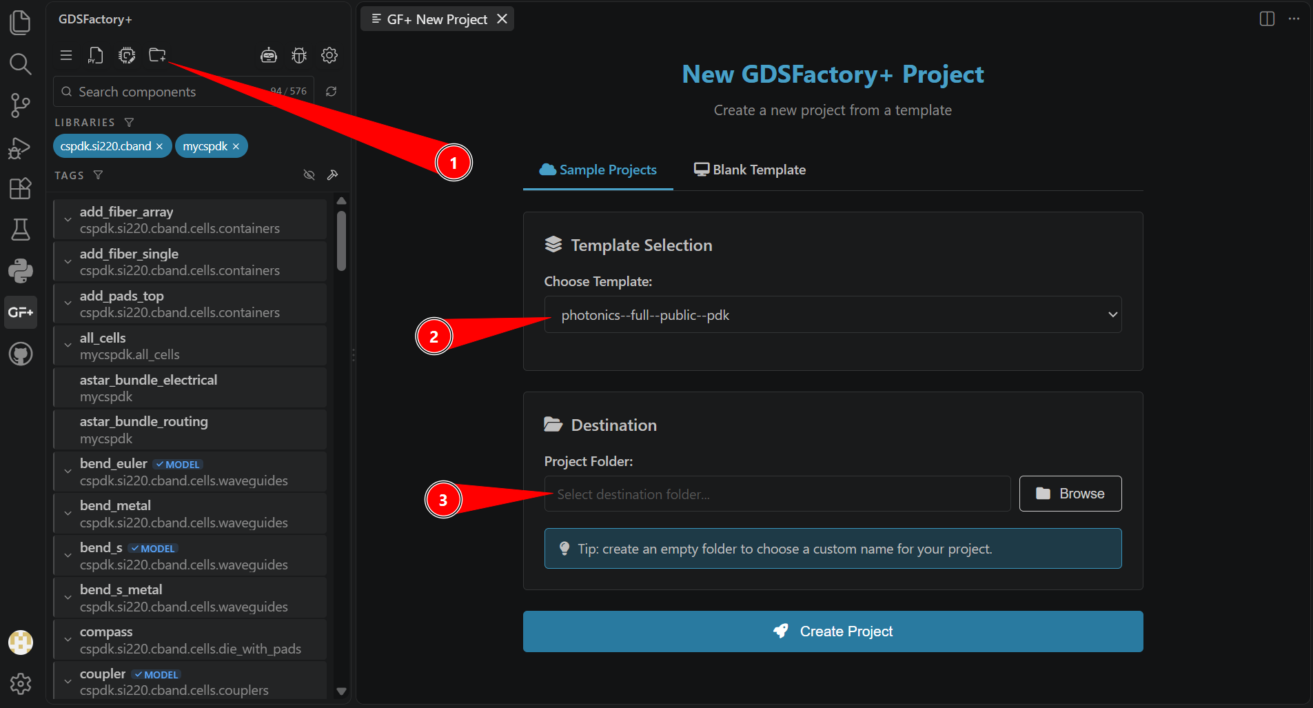
This tutorial uses the photonics-full PDK, a public resource bundled with GDSFactory+. To take full advantage of this tutorial, create a new template project with the New GDSFactory+ Project button at the top of the GF+ sidebar, select photonics--full-public--pdk from the list, and customize the destination folder. Then, use 🚀 Create Project to get started!
The following video walks through the same demo, but in an older version of GDSFactory+. The written guide that follows contains the most up-to-date instructions.
The GDSFactory+ Graphical Workflow
GDSFactory+ has three ways of visualizing your photonic, electrical, and quantum RF circuits.
- Schematic Editor allows you to create block diagrams with ideal electrical and optical connections between Component models, without regard to the actual size of the die
- Layout & Routing Editor is a graphical way of laying out your circuit by clicking and dragging Components and routes
- GDS Viewer allows you to preview a built .gds file before sending it to a foundry for fabrication
Under the hood, all the information associated with a circuit's Schematic Editor and Layout & Routing Editor representations are contained in a single .gsch schematic file, which is stored as YAML-style plain text. This means your block diagram and layout are fundamentally connected, and is what makes GDSFactory+ 2.0 so powerful.
Create a schematic file
The first thing to do is create one of these block diagram schematic files.
-
In the GF+ tab, select the
New Schematic (.gsch)button.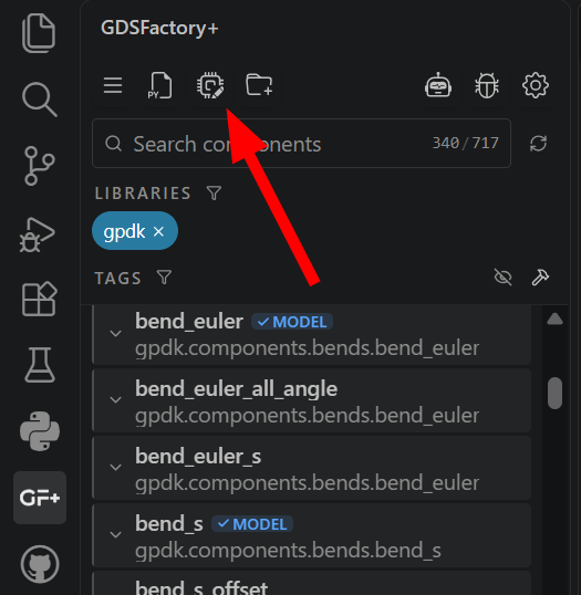
-
Above "Schematic filename" type the name of your new schematic (
rings1for example) and press enter to confirm. This will create a new schematic file namedrings1and open itsSchematic Viewin a new tab.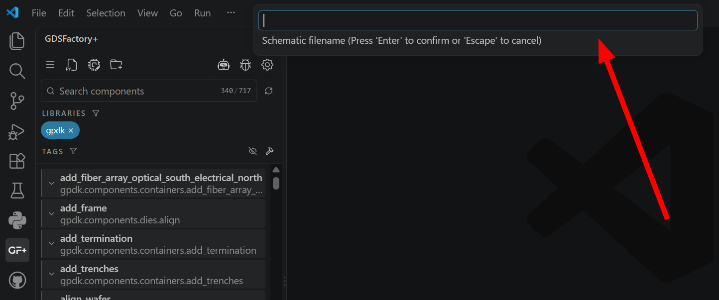
Schematic: Add components and connect them
Let's add two ring resonators and practice optical wiring in the Schematic Editor. Then, we'll adjust and route them in the Layout & Routing Editor.
-
We'll add the rings with the "Add component from library" button at the bottom. Select the component icon, make sure "gpdk" is selected on the left menu, type in "ring_single", then select
ring_single type:cktfrom the right menu. Then simply place the component twice.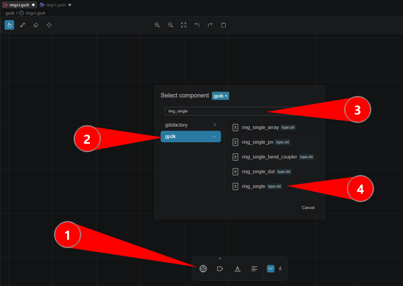
-
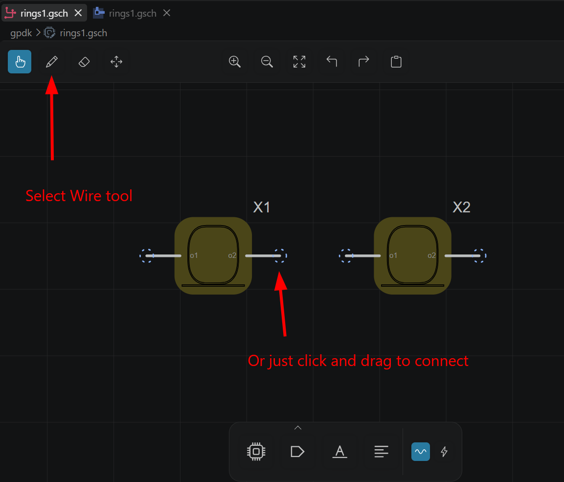
Use the "Wire" tool on the top left to connect the two rings, or just hover over the exposed o2 port of the left ring and click to drag a wire to the o1 port of the right ring.
-
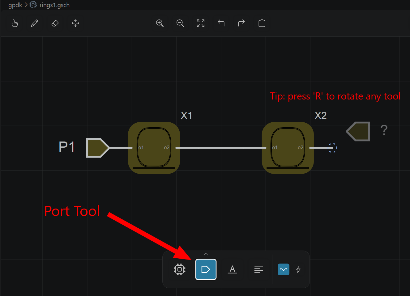
Now let's add ports to your circuit, so we can simulate inputs and outputs later. Select the "Add port" tool on the bottom interface, or press [p]. Then click on the input port. Use the [r] key to rotate the tool, then click on the output port. You should now see port P1 and P2 on either end of your circuit.
Layout: Route optical waveguide connection
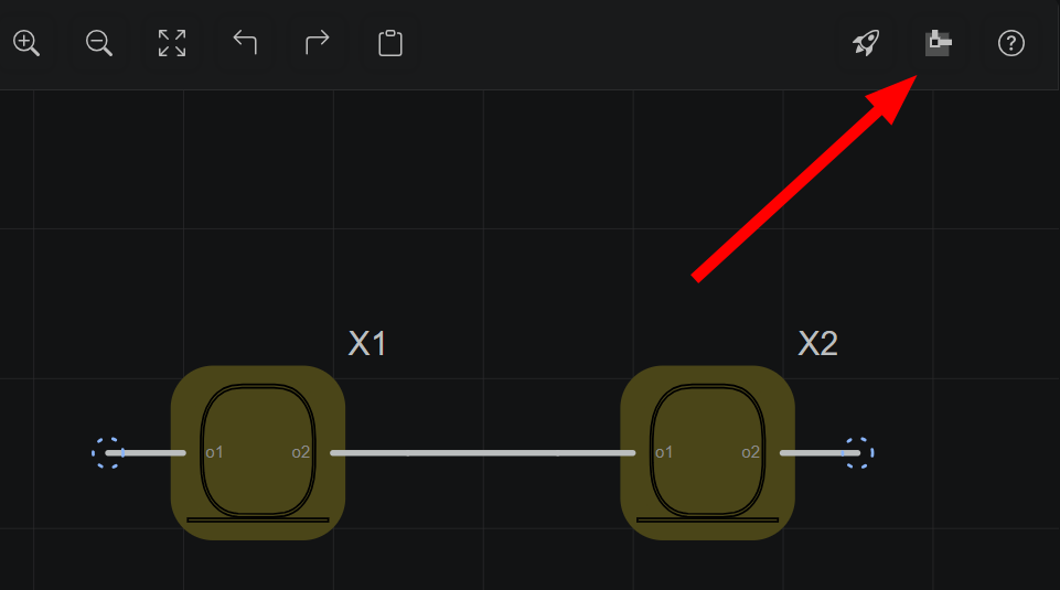
Now it's time to lay out your photonic circuit. Select "Open in layout editor" on the top right.
-
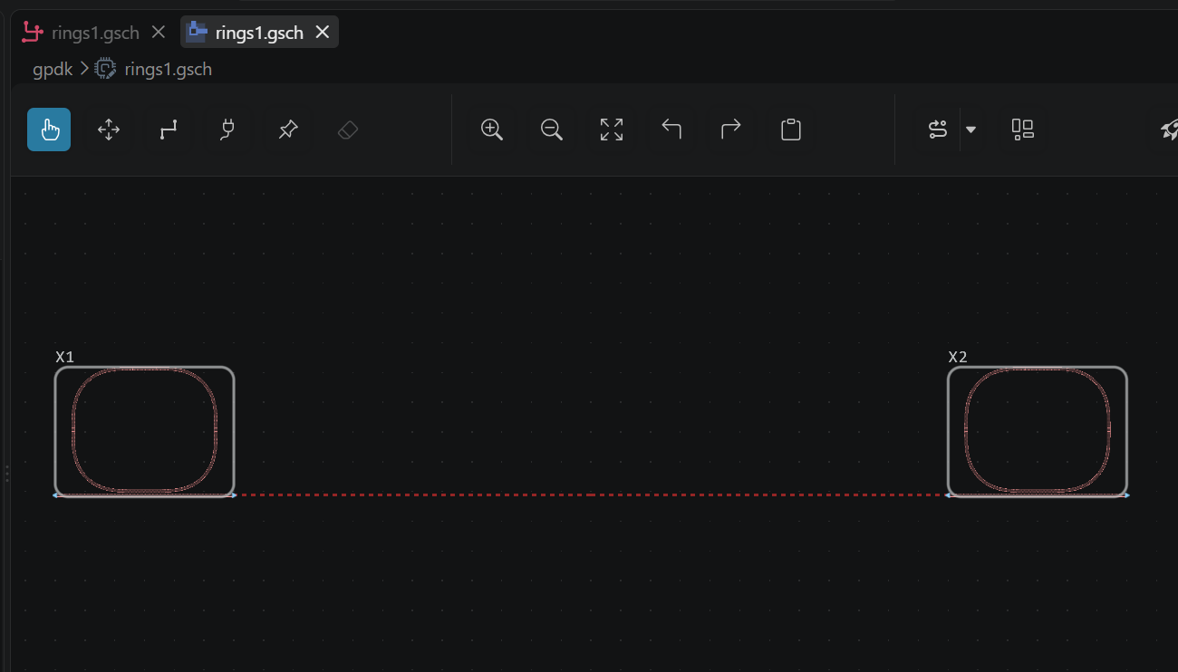
You should see your two ring resonators connected with a ghost wire.
-
You have two options for routing: either manually click and drag between the appropriate ports with the Route tool in the top left (exactly the same as with the Wire tool earlier!), or let GF+ auto-route by right clicking the ghost wire or selecting "Auto Route" in the top right.
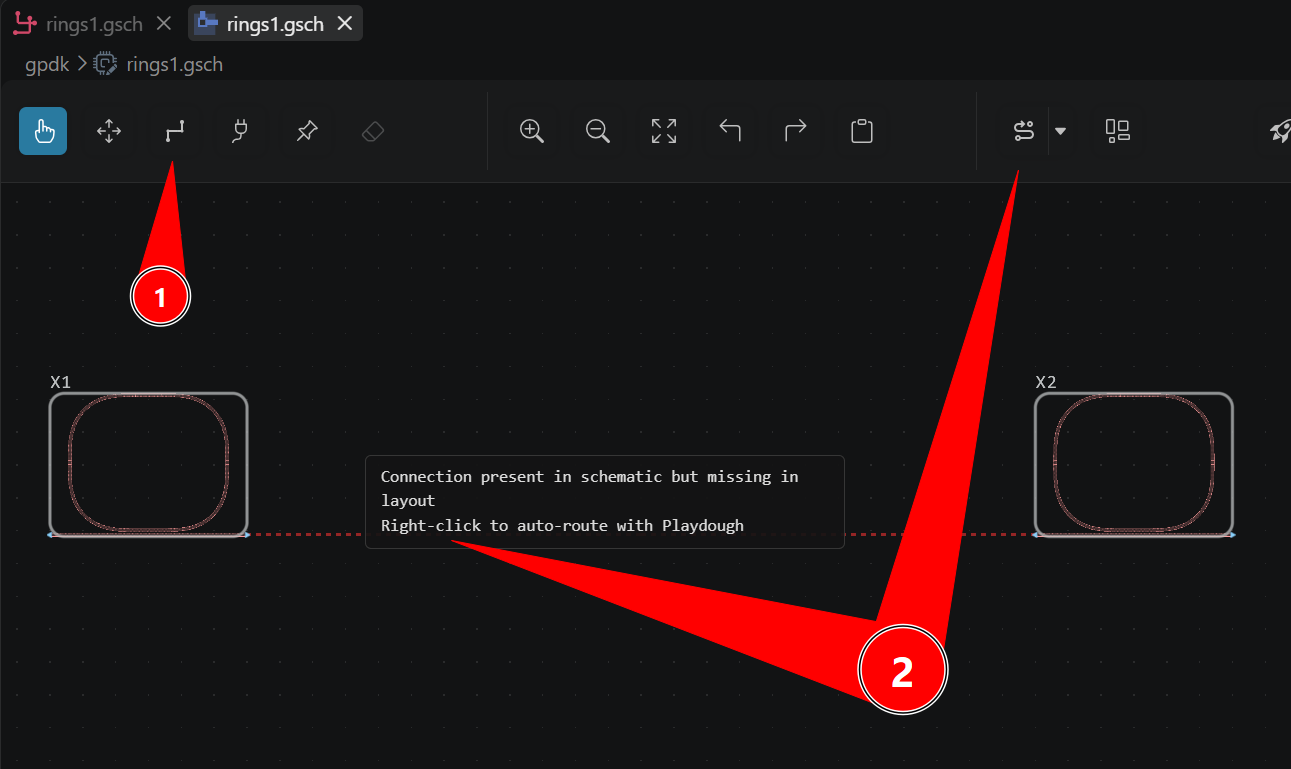
If you run into any issues with the auto-router, try toggling "Finetune" in the auto route dropdown menu > Route settings.
-
Now you can build your layout's GDS and view it with the built in GDS viewer; just select the hammer icon on the top right of the Layout Editor and the GDS should pop up in a new window.
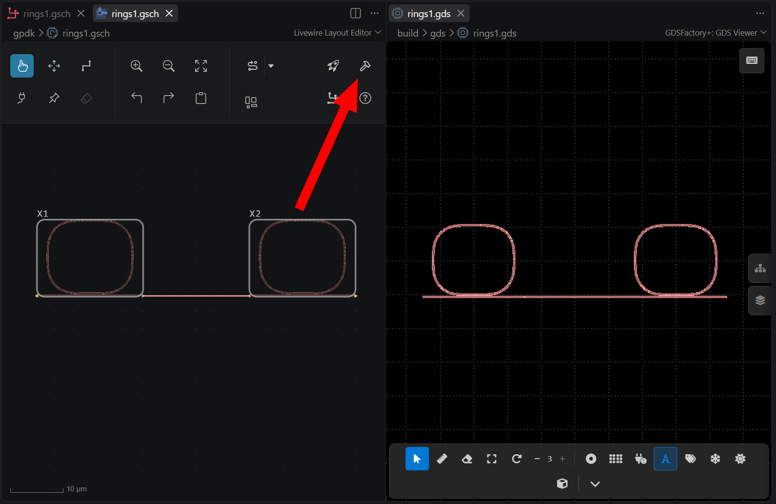
Congratulations! You've now designed and laid out your first photonic circuit with GDSFactory+!
Simulate the circuit
In order to make sure your circuit works as intended, let's run a simple wavelength sweep simulation on the two rings. Luckily, you've already placed your input and output ports; in your own designs, make sure to include ports wherever you need optical or electrical I/O.
-
In the right top bar of the Schematic or Layout Editor, click the button with the rocket
🚀icon. This should open the simulation window, with a few default values automatically provided.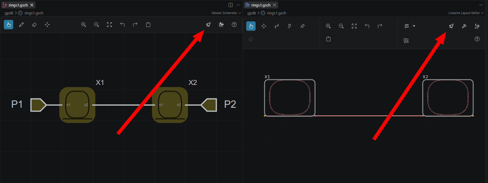
You can select the Simulation tool from either the Schematic or Layout editor.
-
These defaults should be sufficient for our purposes; go ahead and press the
▷ Simulatebutton to see your results.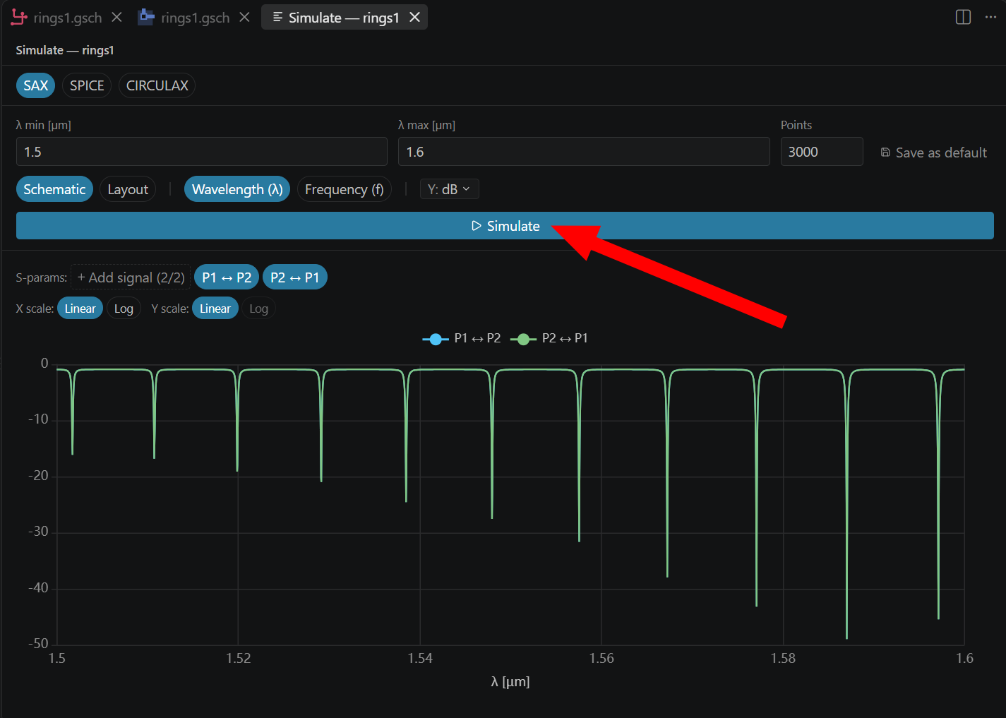
Optionally, try toggling "Layout" to "Schematic" on the top left of the
▷ Simulatebutton. In this particular case the layout and schematic are functionally identical (the path length between the rings doesn't introduce any additional physics effects) so they should look the same, but this may not hold true in more complicated circuits.
Understanding the simulation results
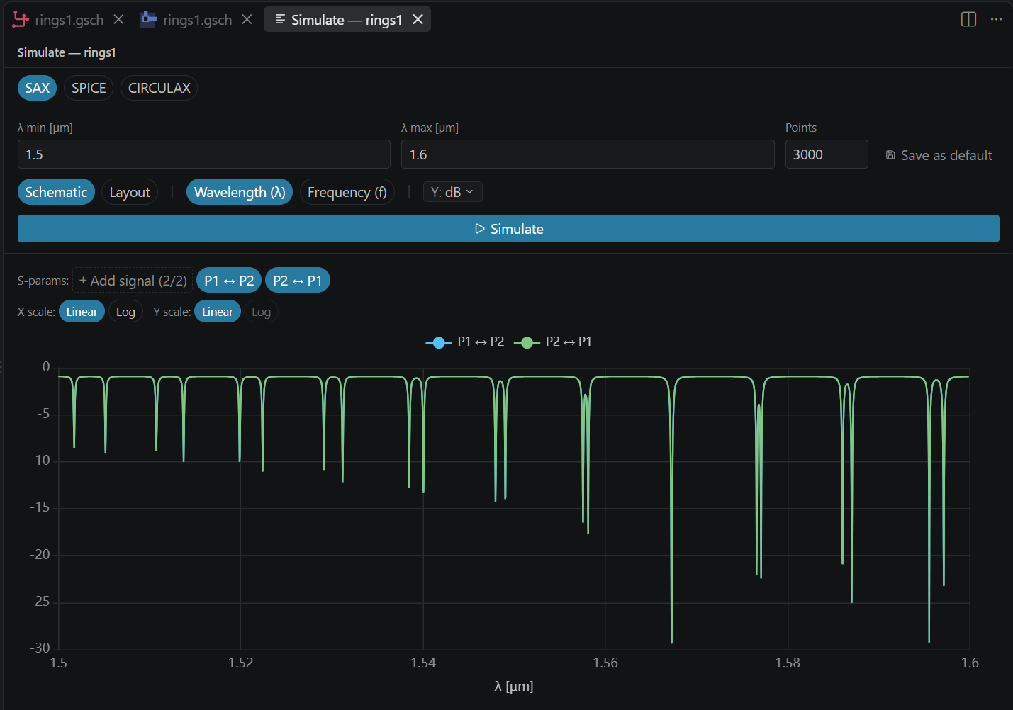
Under the hood, the default radius for the ring_single gpdk component is 10μm, so both rings are filtering the exact same wavelengths. Now, back in the Schematic Editor let's try explicitly setting the two rings' radii to different values, say to 10μm and 11μm. This should result in a different resonance pattern for our photonic circuit.
Click on the Schematic Editor window, then right click the ring components to change their radius values.
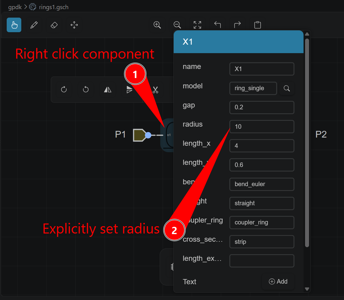
Be aware, when you change values in the schematic, your layout auto-updates to match. Now if you visit the Layout Editor, you'll see the rings are misaligned, since you've made one of them larger, and the route was expecting a perfectly horizontal manhattan route between the two.
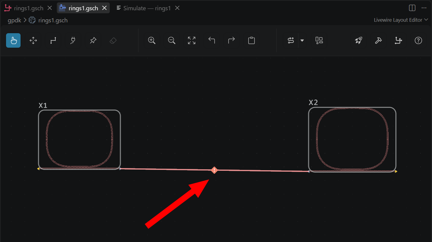
Now is a good time to practice adjusting your layout. GDSFactory+ Layout Editor features a handy snap-to-grid function that helps you align components based on their port locations horizontally and vertically. Try clicking and dragging the right ring until the blue lock icon snaps your mouse and the component exactly in line with the left component.
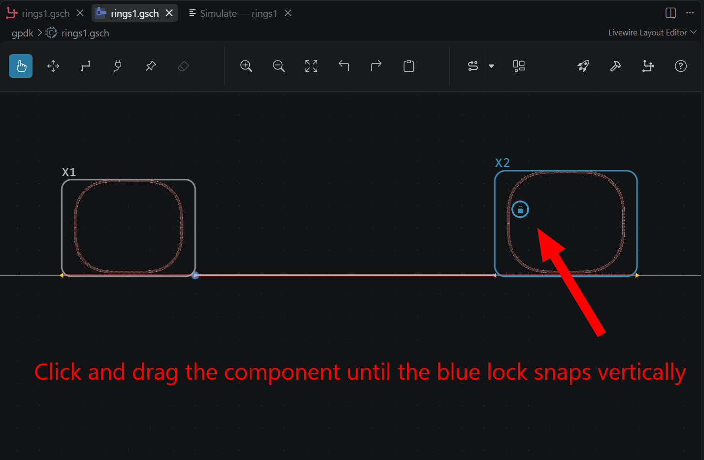
Now you have two rings with different radii, and thus they should filter slightly different wavelengths (and have different FSRs). Indeed, if you re-run the simulation now they have two different resonance patterns.
Conclusion
In this tutorial, you designed, laid out, simulated and iterated on a simple two-ring system, all far quicker than you could with legacy EDA tools. Continue to the next step to see how GSDF+ can also help with layout verification.
Continue to Step 3a: Check for Design Errors - DRC
Optional: For more design and simulation, continue to Advanced Workflow: Layout Aware Design with Grating Couplers
Appendix: Additional info about component loading
Note about lazy loading
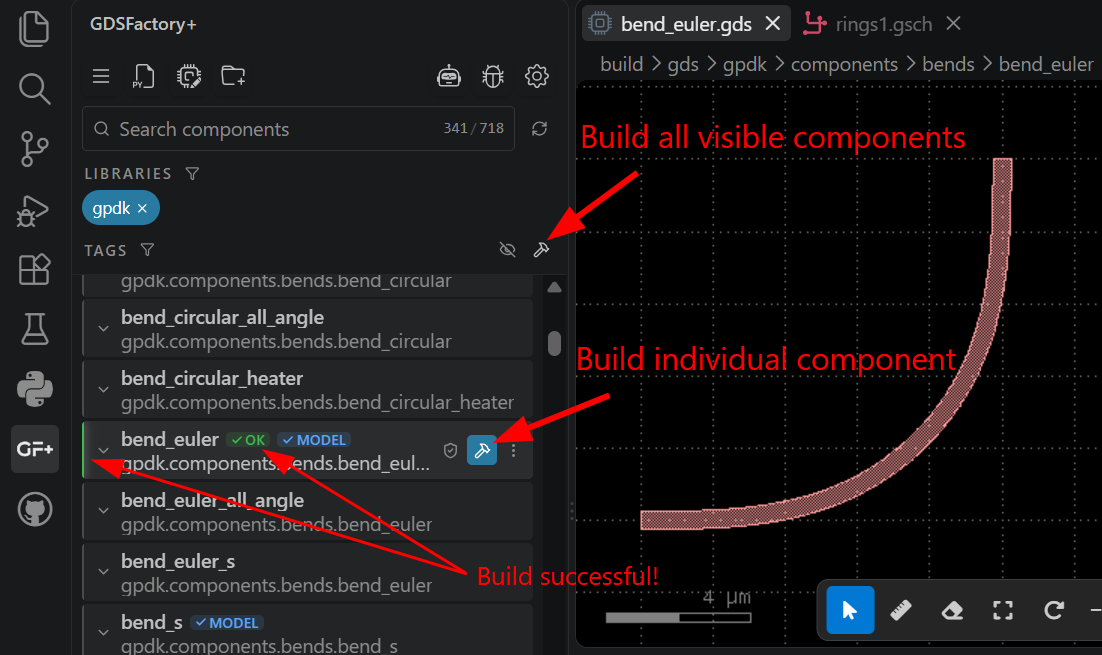
Component GDS files are built when needed; in other words, they are lazy loaded. To manually build a component, select the hammer icon on the component listing, or select the hammer icon on the header to build all currently-visible components (this may take awhile for large projects). You'll know it was successful when you see a green highlight to the left of the component listing, and ✓ OK to the right of the component's name.
Note about models
All shown components in the list have an associated .gds file that can be built, but the ✓ MODEL tag means that the component has both a layout and an ideal schematic-side simulation model associated with it.
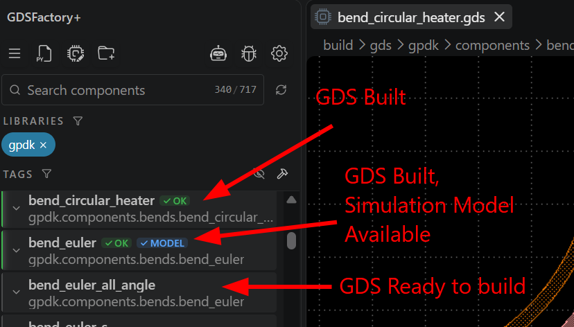
Note that some hierarchical components may not show ✓ MODEL, but you might still be able to simulate them if their components with models are used in the hierarchy.