Step 2: Design an Electrical Circuit
In this step, we'll design and simulate a simple electrical circuit using GDSFactory+ 2.0. For this tutorial you can use any PDK or project file, as we'll only be using ideal electrical components to familiarize ourselves with the schematic interface.
Introduction to Schematic Editor
The first step is to create your schematic. Select the "New Schematic (.gsch)" button in the GF+ tab to get started.
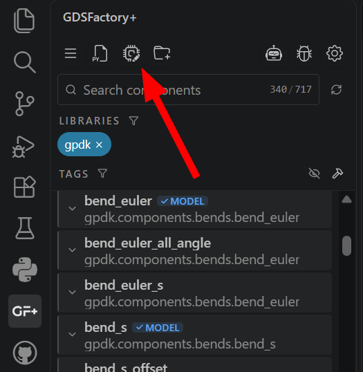
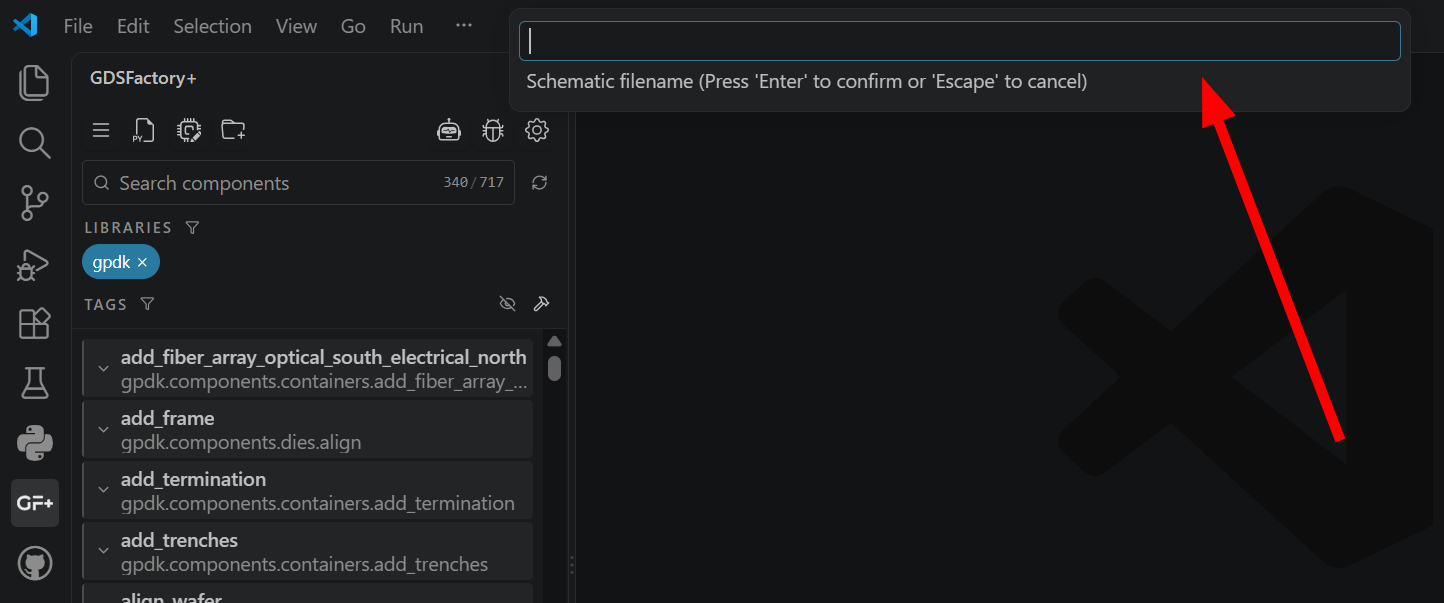
In the pop-up, enter a name for your new schematic, for example test_electrical.
You should now see an empty schematic. Select the "Electrical" tab on the bottom bar to switch from Optical mode to Electrical mode.
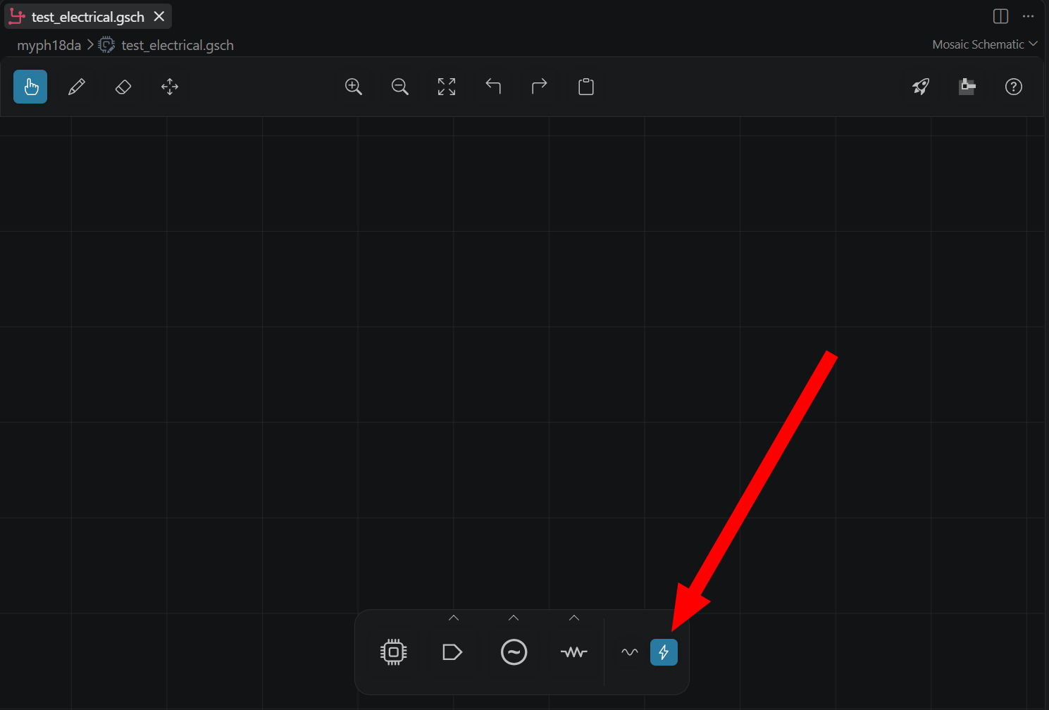
Now in a real design, you would add your own components using the Component Selector tool on the left of the toolbar. However, for PDK compatibility in this tutorial we will use ideal components that are available at all times.
These ideal components are divided into three categories. First, you have node tools, that help you notate power supply lines, gnd connections, and custom labelling nodes as "ports".
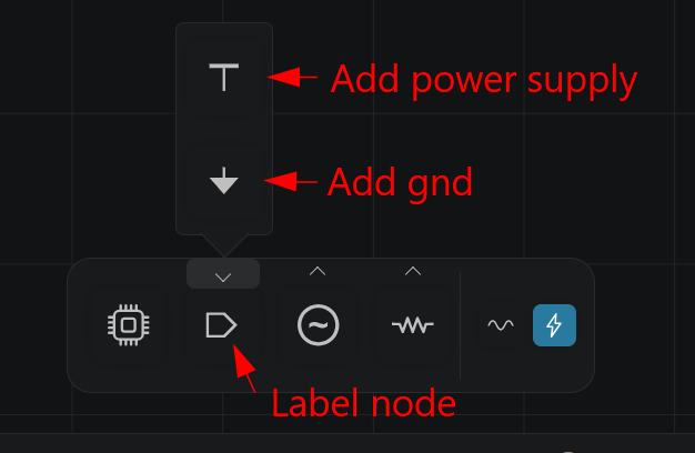
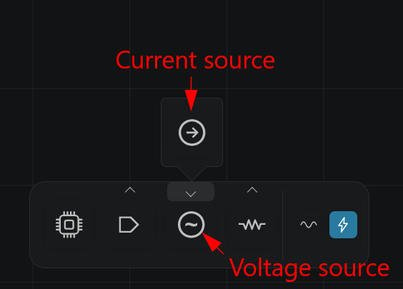
The next category is your standard Voltage and Current sources. You can use these for AC and transient analysis of your circuit.
The last category is passive components: Capacitors, Inductors and Resistors, all customizable per-instance.
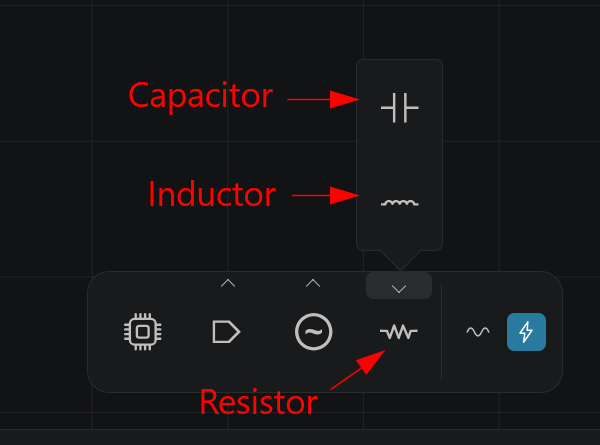
Note that when you do select a new component it will replace the category of tool (so a Capacitor will replace the Resistor in the toolbar until you manually select Resistor again from the dropdown). This allows you to quickly place all the components of the same type.
Design your circuit
Now let's place all three components required for a simple low-pass filter. Add a voltage source, a resistor, and a capacitor in a small loop. You can use the [r] key to rotate a component before you place it.
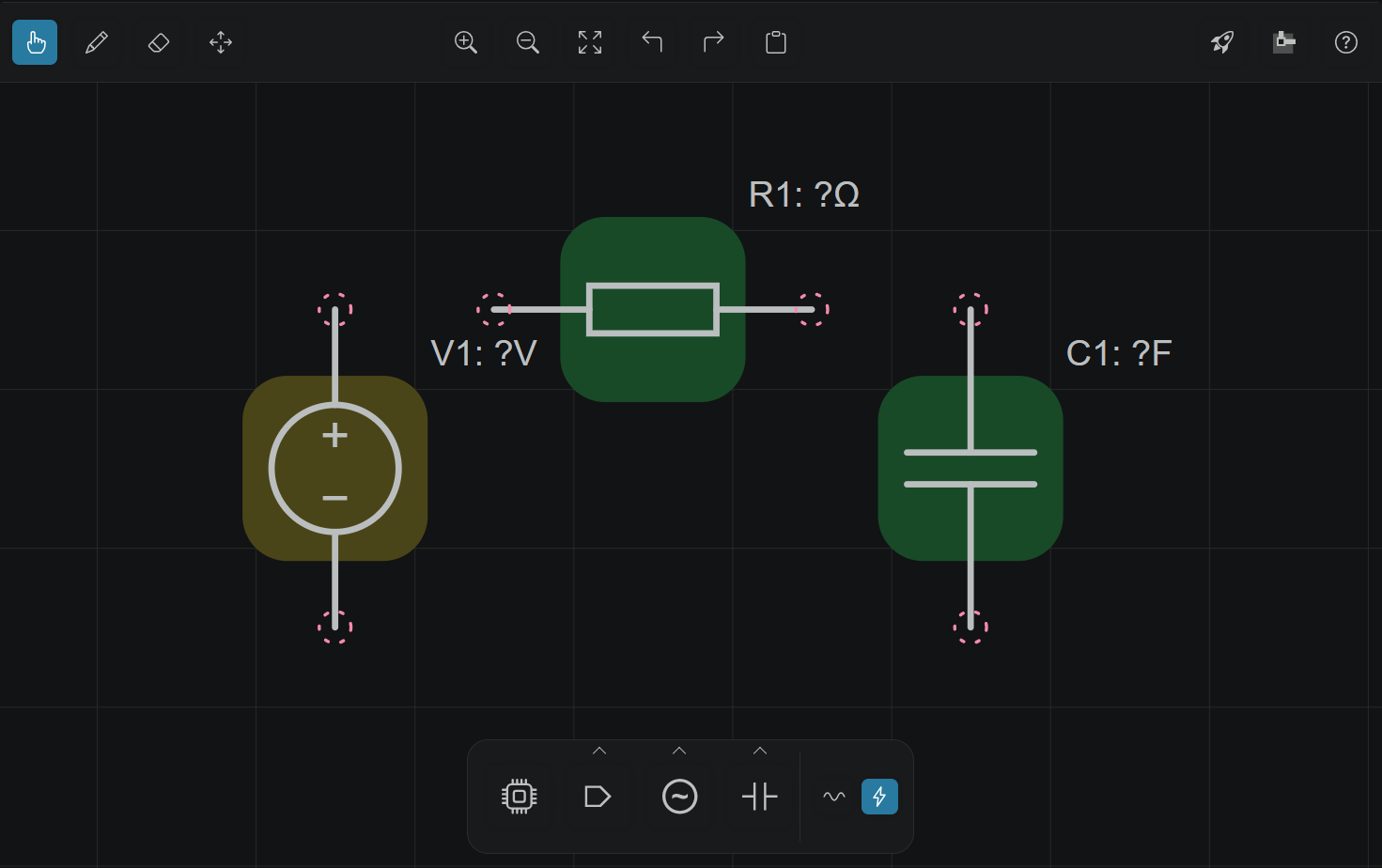
Then use the wiring tool (in the top left or with [w]) or simply click and drag to connect the exposed ports of each component.
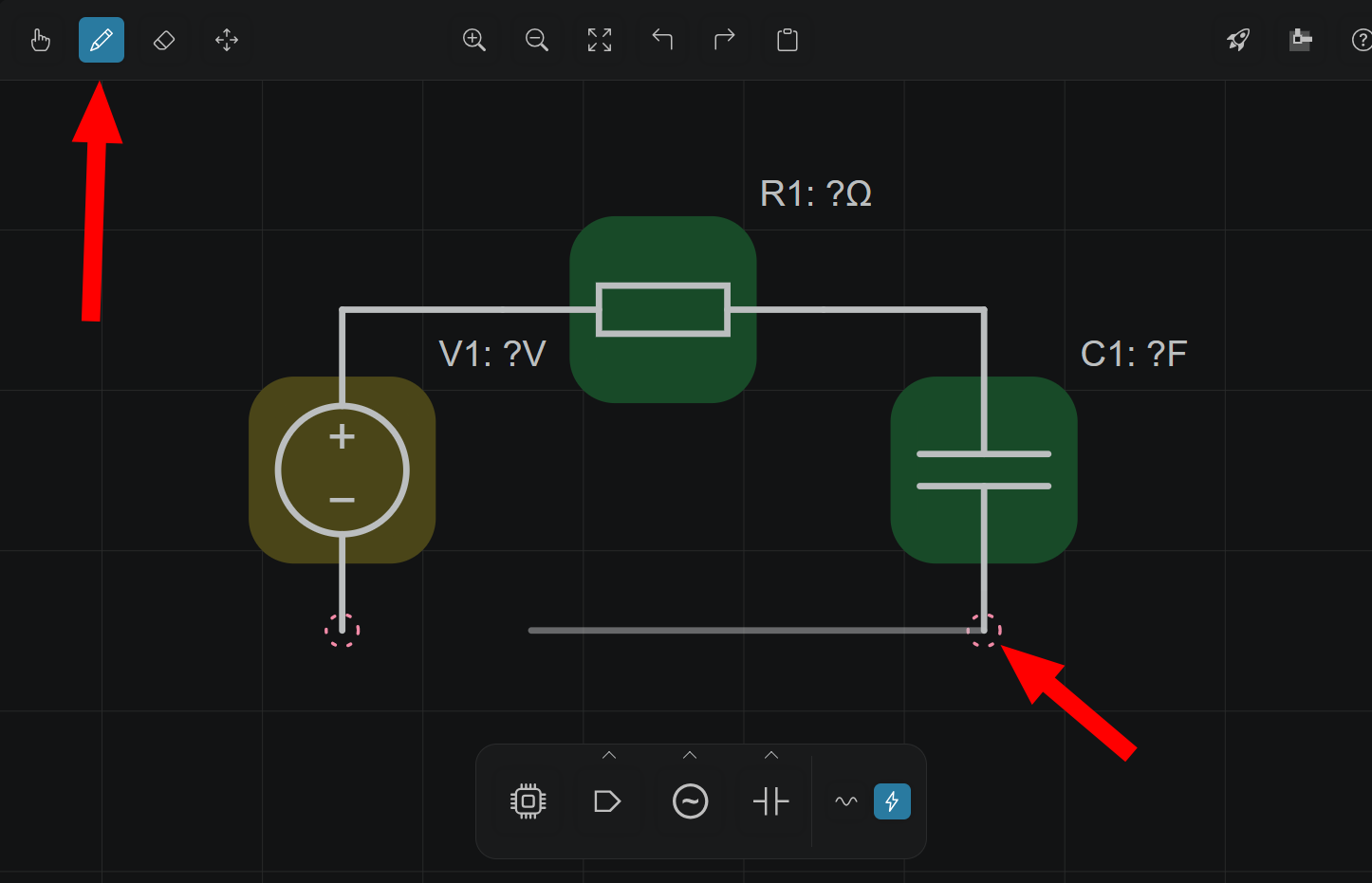
Note: GDSFactory+ automatically differentiates between electrical and optical routes! You can tell these are electrical components because of the pink outline of the circles. Make sure not to mix optical and electrical connections.
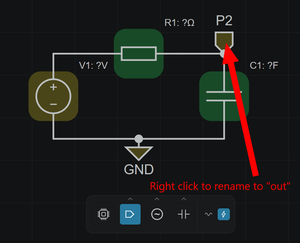
Now let's add a gnd node at the bottom, and also an "out" port on the top right that the simulator will be able to see. Use the right-click menu on the port instance to change its name.
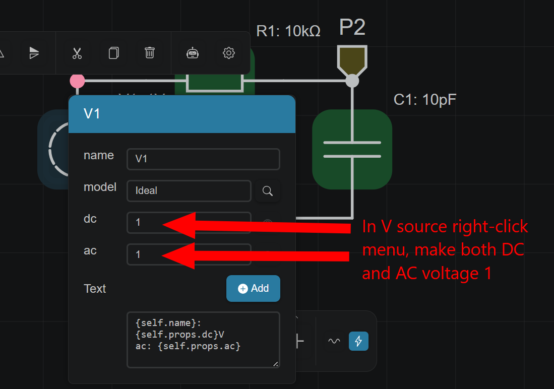
Then just add values to each of the components, also through the right-click menu for each. In this demo, we'll use 10k for the resistance, 10p for the capacitor, and 1V for both DC and AC values of the voltage source.
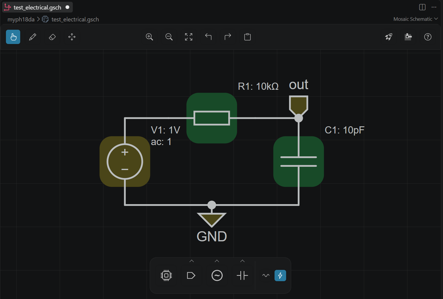
Finished schematic
Once your design is complete, it should look like the following:
Simulating the schematic
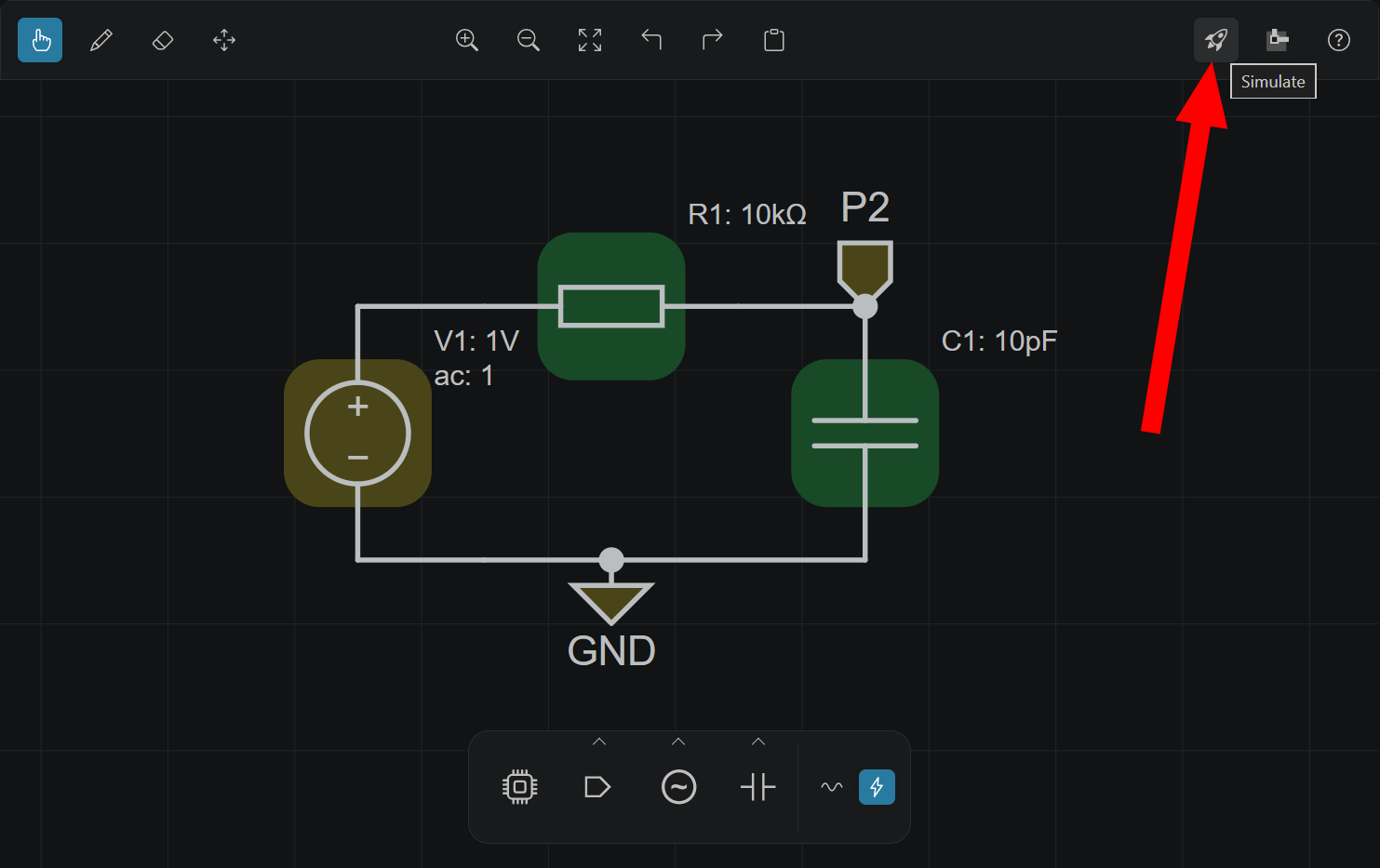
Now let's select the simulation tool on the top right.
Enter the following test parameters to check our circuit's AC response.
- Select SPICE on top bar
- Select AC analysis
- Enter 100kHz (100000) start frequency
- Enter 10MHz (10000000) stop frequency
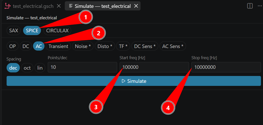
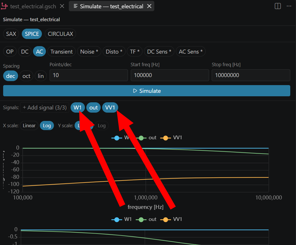
Then select Simulate. Just one last step before we can see our results, click on the W1 and VV1 traces so they don't show up on the output magnitude and phase plots.
Circuit analysis
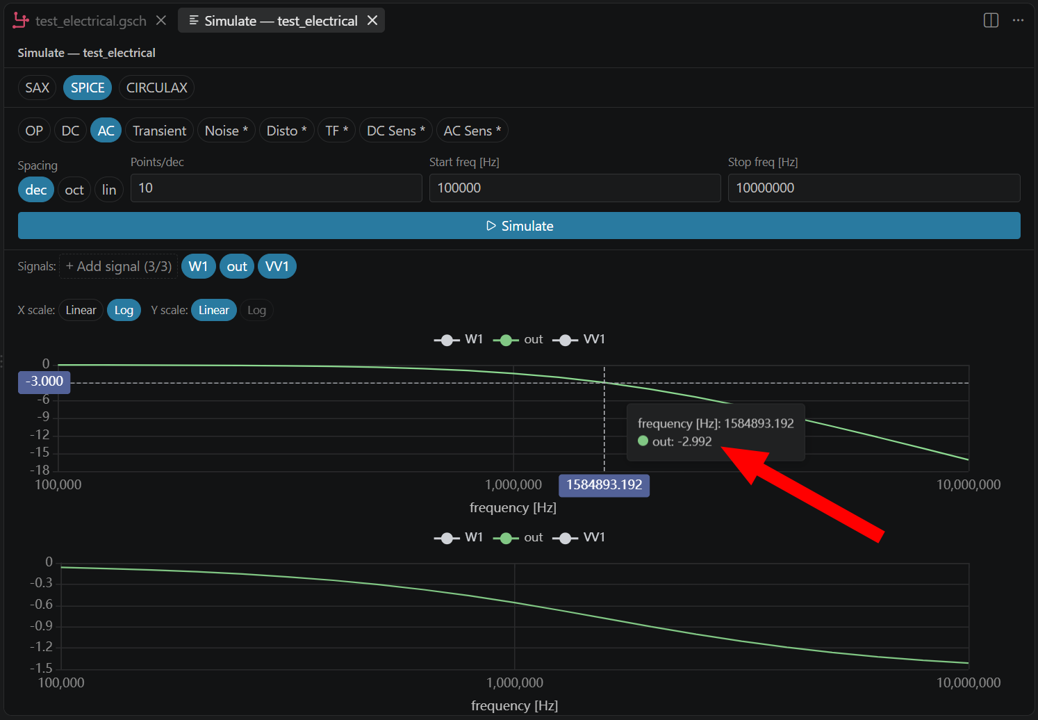
The simulation shows the 3dB cutoff at 1.58 MHz, which corresponds to 10M rad/sec. This is what we expect from a ω0 = 1/RC cutoff frequency with R = 10k and C = 10p.
Conclusion
Congratulations! In this tutorial you simulated a simple RC lowpass circuit in GDSFactory+ and verified its frequency response with a SPICE simulation.
Because these components were all ideal, you weren't able to experiment with the rich GDSFactory+ ecosystem of layout editing, DRC and LVS:
- To get started on layout, try Step 2a: Design a Photonic Circuit or Step 2c: Design a Quantum RF Circuit.
- See Step 3a: Check for Design Errors - DRC for an introduction to DRC.
- See Step 3b: Check for Connectivity Errors - LVS for an introduction to LVS.