Mode Solver Simulations
Learn how to simulate waveguide modes using finite-element FEM and FDFD solvers together with GDSFactory+.
FEM mode solver
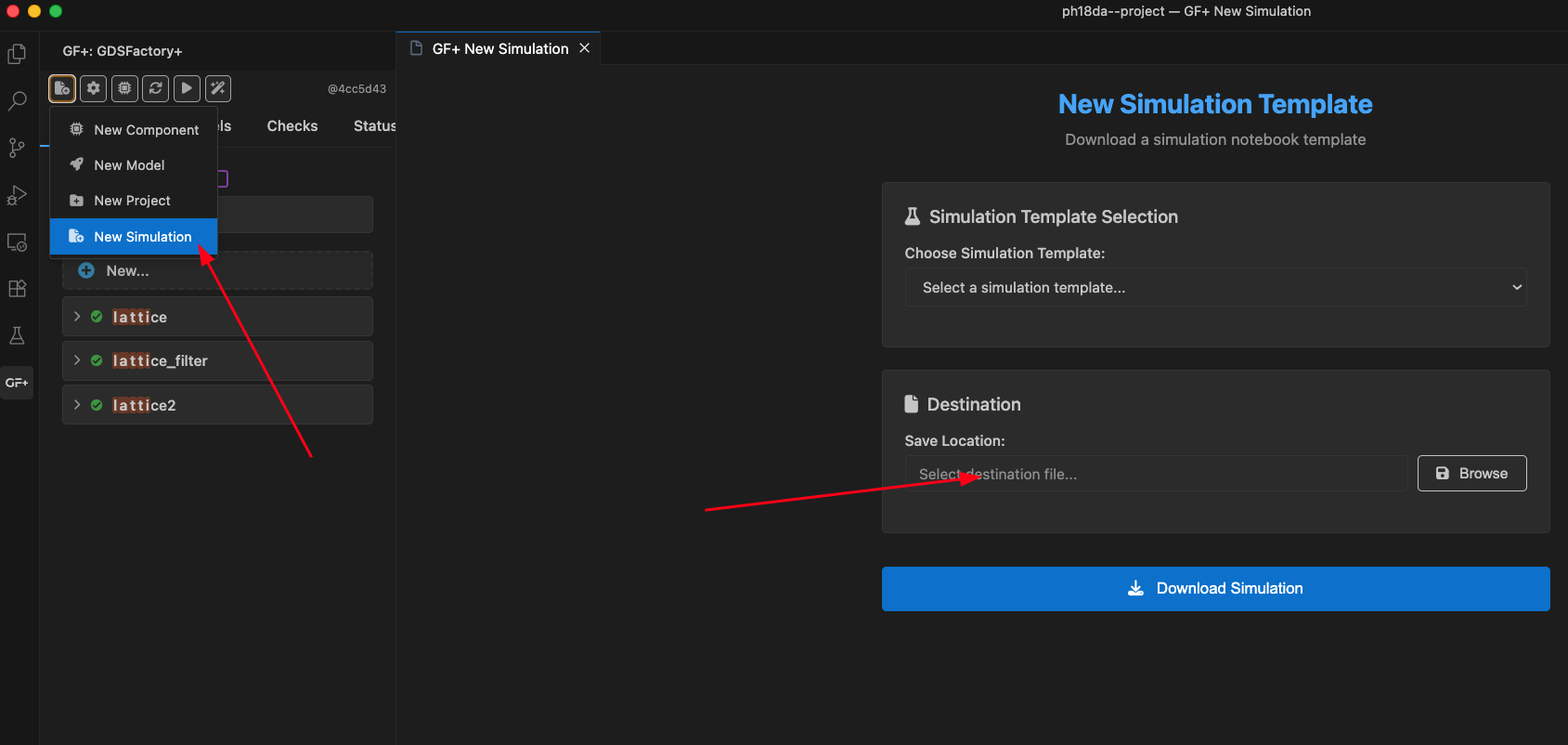
Go to New Simulation:
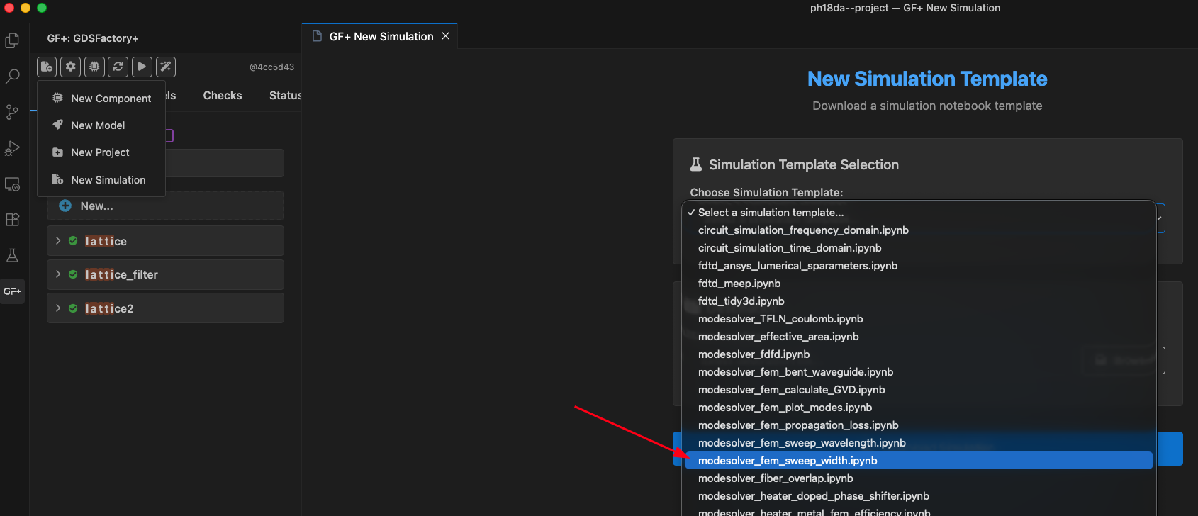
Select the modesolver_fem_sweep_width notebook and click Download Simulation:
Exercises
Q1. For a 400 nm thick silicon nitride (SiN) waveguide, what is the maximum width that ensures single-mode (TE) operation?
Q2. For a 220 nm thick silicon waveguide, what is the maximum width that ensures single-mode (TE) operation?
Q3. Data center photonics often operate in the O-band (~1.3 um) rather than the C-band (~1.55 um). As the wavelength decreases, how does the maximum single-mode width change? Specifically, what is the maximum width for a 220 nm thick silicon waveguide at 1.3 um to remain single-mode (TE)?
We also have an interactive mode solver you can try.
Thermal phase shifter
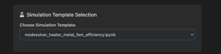
Download modesolver_fem_sweep_width:
Run with heater_width = 2 and notice how you get around 5 radians phase shift.
Q4. As the heater width increases, a larger fraction of the generated heat spreads laterally, reducing the thermal overlap with the target waveguide. What would be a more optimal heater width to improve the overlap between the heat distribution and the waveguide mode?
Q5. The buried oxide (BOX) layer acts as a thermal pathway for the heater. How does the phase shift change when the BOX thickness is reduced (e.g., to 2 um)?
FDFD mode solver
Exercises
Q1. There is a trade-off between bend radius and optical loss: increasing the bend radius reduces mode mismatch (bend loss), but also increases the total propagation length (and thus propagation loss). At what point does increasing the bend radius no longer provide a net benefit — for example, in the context of a Silicon 220 nm waveguide at 1550 nm?
From FDTD to S-parameter model
Run the simulation of a grating coupler in 2D FDTD and create a model, then turn it into a simulation model: