Running Palace Simulations: Mach Zehnder Modulator
Palace is an open-source 3D electromagnetic simulator supporting eigenmode, driven (S-parameter), and electrostatic simulations. This notebook demonstrates using the gsim.palace API to run a driven simulation on a Mach Zehnder Modulator.
Requirements:
- GDSFactory+ account for cloud simulation
Generate layout for MZM
import gdsfactory as gf
import klayout.db as kdb

gf.gpdk.PDK.activate()


def t_shape_dpoly(w1: float, w2: float, h1: float, h2: float) -> kdb.DPolygon:
    w3 = (w2 - w1) / 2
    return kdb.DPolygon(
        [
            kdb.DPoint(-w1 / 2, 0),
            kdb.DPoint(w1 / 2, 0),
            kdb.DPoint(w1 / 2, h1),
            kdb.DPoint(w1 / 2 + w3, h1),
            kdb.DPoint(w1 / 2 + w3, h1 + h2),
            kdb.DPoint(-w1 / 2 - w3, h1 + h2),
            kdb.DPoint(-w1 / 2 - w3, h1),
            kdb.DPoint(-w1 / 2, h1),
        ]
    )


def cpw_conductor(
    layer: tuple[int, int],
    gap: float,
    trace_width: float,
    ground_width: float,
    number_of_ts: int,
    w1: float,
    w2: float,
    h1: float,
    h2: float,
    t_spacing: float,
    port_length: float,
) -> gf.Component:
    comp = gf.Component()
    board_width = trace_width + 2 * ground_width + 2 * gap
    board_length = number_of_ts * (w2 + t_spacing) + t_spacing + port_length * 2
    midwidth = board_width / 2
    x_start = port_length + t_spacing

    def dpoly_to_ipoly(dp: kdb.DPolygon) -> kdb.Polygon:
        dbu = comp.kcl.dbu
        return dp.to_itype(dbu)

    trace = kdb.Region()
    rect_trace = kdb.DPolygon(
        [
            kdb.DPoint(0, midwidth - trace_width / 2),
            kdb.DPoint(board_length, midwidth - trace_width / 2),
            kdb.DPoint(board_length, midwidth + trace_width / 2),
            kdb.DPoint(0, midwidth + trace_width / 2),
        ]
    )
    trace.insert(dpoly_to_ipoly(rect_trace))

    for i in range(number_of_ts):
        dp = t_shape_dpoly(w1, w2, h1, h2)
        dp = dp.transformed(
            kdb.DTrans(
                x_start + i * (w2 + t_spacing) + w2 / 2, midwidth + trace_width / 2
            )
        )
        trace.insert(dpoly_to_ipoly(dp))

    for i in range(number_of_ts):
        dp = t_shape_dpoly(w1, w2, h1, h2)
        dp = dp.transformed(kdb.DTrans(kdb.DTrans.R180))
        dp = dp.transformed(
            kdb.DTrans(
                x_start + i * (w2 + t_spacing) + w2 / 2, midwidth - trace_width / 2
            )
        )
        trace.insert(dpoly_to_ipoly(dp))

    trace.merge()
    comp.add_polygon(trace, layer=layer)

    ground_lower = kdb.Region()
    rect_gL = kdb.DPolygon(
        [
            kdb.DPoint(0, midwidth - trace_width / 2 - gap),
            kdb.DPoint(0, midwidth - trace_width / 2 - gap - ground_width),
            kdb.DPoint(board_length, midwidth - trace_width / 2 - gap - ground_width),
            kdb.DPoint(board_length, midwidth - trace_width / 2 - gap),
        ]
    )
    ground_lower.insert(dpoly_to_ipoly(rect_gL))

    for i in range(number_of_ts):
        dp = t_shape_dpoly(w1, w2, h1, h2)
        dp = dp.transformed(
            kdb.DTrans(
                x_start + i * (w2 + t_spacing) + w2 / 2,
                midwidth - trace_width / 2 - gap,
            )
        )
        ground_lower.insert(dpoly_to_ipoly(dp))

    ground_lower.merge()
    comp.add_polygon(ground_lower, layer=layer)

    ground_upper = kdb.Region()
    rect_gU = kdb.DPolygon(
        [
            kdb.DPoint(0, midwidth + trace_width / 2 + gap),
            kdb.DPoint(0, midwidth + trace_width / 2 + gap + ground_width),
            kdb.DPoint(board_length, midwidth + trace_width / 2 + gap + ground_width),
            kdb.DPoint(board_length, midwidth + trace_width / 2 + gap),
        ]
    )
    ground_upper.insert(dpoly_to_ipoly(rect_gU))

    for i in range(number_of_ts):
        dp = t_shape_dpoly(w1, w2, h1, h2)
        dp = dp.transformed(kdb.DTrans(kdb.DTrans.R180))
        dp = dp.transformed(
            kdb.DTrans(
                x_start + i * (w2 + t_spacing) + w2 / 2,
                midwidth + trace_width / 2 + gap,
            )
        )
        ground_upper.insert(dpoly_to_ipoly(dp))

    ground_upper.merge()
    comp.add_polygon(ground_upper, layer=layer)

    return comp


def rib(
    layer: tuple[int, int],
    board_width: float,
    board_length: float,
    gap: float,
    trace_width: float,
    opt_width: float,
    port_length: float,
    t_spacing: float,
) -> gf.Component:
    rib_comp = gf.Component()
    midwidth = board_width / 2
    center = midwidth + trace_width / 2 + gap / 2
    offset = port_length + t_spacing
    rib_comp.add_polygon(
        [
            (offset, center - opt_width / 2),
            (board_length - offset, center - opt_width / 2),
            (board_length - offset, center + opt_width / 2),
            (offset, center + opt_width / 2),
        ],
        layer=layer,
    )
    center = midwidth - trace_width / 2 - gap / 2
    rib_comp.add_polygon(
        [
            (offset, center - opt_width / 2),
            (board_length - offset, center - opt_width / 2),
            (board_length - offset, center + opt_width / 2),
            (offset, center + opt_width / 2),
        ],
        layer=layer,
    )
    return rib_comp


def mach_zehnder_cpw(
    conductor_layer,
    gap: float,
    trace_width: float,
    ground_width: float,
    rib_width: float,
    number_of_ts: int,
    t_w1: float,
    t_w2: float,
    t_h1: float,
    t_h2: float,
    t_spacing: float,
    port_length: float,
) -> gf.Component:
    comp = gf.Component()
    board_width = trace_width + 2 * ground_width + 2 * gap
    board_length = number_of_ts * (t_w2 + t_spacing) + t_spacing + port_length * 2
    cpw_comp = cpw_conductor(
        layer=conductor_layer,
        gap=gap,
        trace_width=trace_width,
        ground_width=ground_width,
        number_of_ts=number_of_ts,
        w1=t_w1,
        w2=t_w2,
        h1=t_h1,
        h2=t_h2,
        t_spacing=t_spacing,
        port_length=port_length,
    )
    comp.add_ref(cpw_comp)

    # Commented for now
    # rib_comp = rib(
    #     layer=tfln_rib_layer.gds_layer,
    #     board_width=board_width,
    #     board_length=board_length,
    #     gap=gap,
    #     trace_width=trace_width,
    #     opt_width=rib_width,
    #     port_length=port_length,
    #     t_spacing=t_spacing,
    # )
    # comp.add_ref(rib_comp)

    midwidth = board_width / 2

    comp.add_port(
        name="o1",
        center=(0, midwidth),
        width=gap,
        orientation=180,
        port_type="electrical",
        layer=conductor_layer,
    )
    comp.add_port(
        name="o2",
        center=(board_length, midwidth),
        width=gap,
        orientation=0,
        port_type="electrical",
        layer=conductor_layer,
    )
    return comp


# T-shape parameters
number_of_ts = 1
w1 = 2  # width of the stem of the T
w2 = 45  # width of the T top bar
h1 = 6  # height of the stem of the T
h2 = 2  # height of the T top bar
spacing = 5  # spacing between Ts
trace_width = 100
ground_width = 300
MZM_CPW_GAP = 5 + 2 * (h1 + h2)  # gap + 2*(h1+h2) to ensure T shapes dont overlap

PORT_LENGTH = 10  # length of the port

mzm_cpw_comp = mach_zehnder_cpw(
    conductor_layer=gf.gpdk.LAYER.M3,
    gap=MZM_CPW_GAP,
    trace_width=trace_width,
    ground_width=ground_width,
    rib_width=1,
    number_of_ts=number_of_ts,
    t_w1=w1,
    t_w2=w2,
    t_h1=h1,
    t_h2=h2,
    t_spacing=spacing,
    port_length=PORT_LENGTH,
)

# Draw and plot MZM CPW component
_mzm_cpw_comp = mzm_cpw_comp.copy()
_mzm_cpw_comp.draw_ports()
_mzm_cpw_comp.plot()
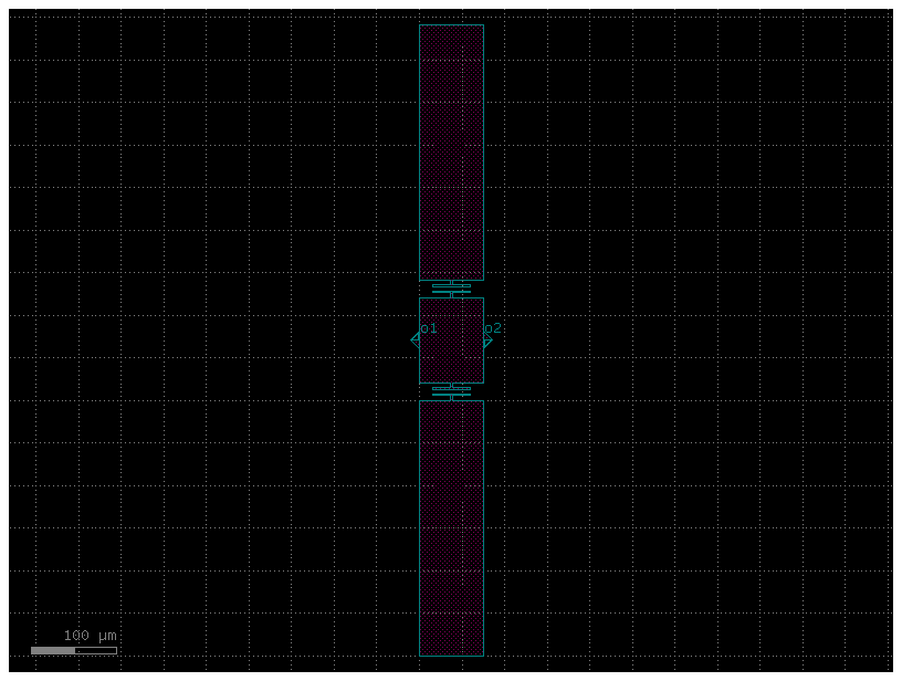
Configure and run simulation with DrivenSim
from gsim.palace import DrivenSim

# Create simulation object
sim = DrivenSim()

# Set output directory
sim.set_output_dir("./palace-sim-mzm")

# Set the component geometry
sim.set_geometry(mzm_cpw_comp)
sim.set_stack()
sim.set_airbox(margin_x=50, margin_y=0, z_above=100, z_below=100)

# Configure via ports (Metal1 ground plane to TopMetal2 signal)
# Configure left CPW port (o1)
sim.add_cpw_port(
    "o1", layer="metal3", s_width=trace_width, gap_width=MZM_CPW_GAP, length=PORT_LENGTH
)

# Configure right CPW port (o2)
sim.add_cpw_port(
    "o2", layer="metal3", s_width=trace_width, gap_width=MZM_CPW_GAP, length=PORT_LENGTH
)

# Configure driven simulation (frequency sweep for S-parameters)
sim.set_driven(fmin=1e9, fmax=100e9, num_points=40, save_step=20)

# Validate configuration
print(sim.validate_config())
[34m18:12:48[0m | [33m[22mWARNING [0m | [33m[22mpyvirtualdisplay not available; continuing without Xvfb[0m
Validation: PASSED
Mesh Summary
========================================
Dimensions: 275.0 x 742.0 x 207.2 µm
Nodes:      66,553
Elements:   480,146
Tetrahedra: 369,686
Edge length: 0.33 - 53.19 µm
Quality:    0.631 (min: 0.004)
SICN:       0.682 (all valid)
----------------------------------------
Volumes (2):
  - sio2 [1]
  - air [2]
Surfaces (9):
  - metal3_xy [3]
  - metal3_z [4]
  - P1_E0 [5]
  - P1_E1 [6]
  - P2_E0 [7]
  - P2_E1 [8]
  - air__sio2 [9]
  - sio2__None [10]
  - air__None [11]
----------------------------------------
Mesh:   palace-sim-mzm/palace.msh
# Static rendering keeps the mesh visible in the published Markdown.
sim.plot_mesh(
    show_groups=[
        "metal3_xy",
        "metal3_z",
        "P1_E0",
        "P1_E1",
        "P2_E0",
        "P2_E1",
        "SiO2",
        "passive",
    ],
    transparent_groups=["air__None", "air__passive", "SiO2__passive"],
    style="solid",
    interactive=False,
)
[34m18:13:07[0m | [33m[22mWARNING [0m | [33m[22mpyvirtualdisplay not available; continuing without Xvfb[0m
[0m[33m2026-08-20 18:13:07.779 ( 18.961s) [ 7F549F445B80]vtkXOpenGLRenderWindow.:1460 WARN| bad X server connection. DISPLAY=[0m
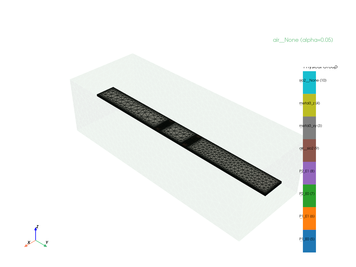
Info    : Reading 'palace-sim-mzm/palace.msh'...
Info    : 66553 nodes
Info    : 469236 elements
Info    : [  0%] Reading elements
Info : [ 10%] Reading elements
Info : [ 20%] Reading elements
Info : [ 30%] Reading elements
Info : [ 40%] Reading elements
Info : [ 50%] Reading elements
Info : [ 60%] Reading elements
Info : [ 70%] Reading elements
Info : [ 80%] Reading elements
Info : [ 90%] Reading elements
Info    : Done reading 'palace-sim-mzm/palace.msh'
Info    : Reading 'palace-sim-mzm/palace.msh'...
Info    : 66553 nodes
Info    : 469236 elements
Info    : [  0%] Reading elements
Info : [ 10%] Reading elements
Info : [ 20%] Reading elements
Info : [ 30%] Reading elements
Info : [ 40%] Reading elements
Info : [ 50%] Reading elements
Info : [ 60%] Reading elements
Info : [ 70%] Reading elements
Info : [ 80%] Reading elements
Info : [ 90%] Reading elements
Info : Done reading 'palace-sim-mzm/palace.msh'
Info : Reading 'palace-sim-mzm/palace.msh'...
Info : 66553 nodes
Info    : 469236 elements
Info    : [  0%] Reading elements
Info : [ 10%] Reading elements
Info : [ 20%] Reading elements
Info : [ 30%] Reading elements
Info : [ 40%] Reading elements
Info : [ 50%] Reading elements
Info : [ 60%] Reading elements
Info : [ 70%] Reading elements
Info : [ 80%] Reading elements
Info : [ 90%] Reading elements
Info : Done reading 'palace-sim-mzm/palace.msh' Info : Reading 'palace-sim-mzm/palace.msh'... Info : 66553 nodes
Info : 469236 elements
Info : [ 0%] Reading elements
Info : [ 10%] Reading elements
Info : [ 20%] Reading elements
Info : [ 30%] Reading elements
Info : [ 40%] Reading elements
Info : [ 50%] Reading elements
Info : [ 60%] Reading elements
Info : [ 70%] Reading elements
Info : [ 80%] Reading elements
Info : [ 90%] Reading elements
Info    : Done reading 'palace-sim-mzm/palace.msh'


PosixPath('palace-sim-mzm/config.json')
Run simulation on GDSFactory+ Cloud
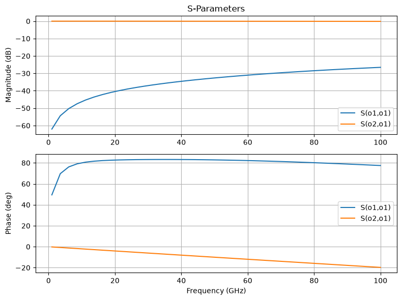
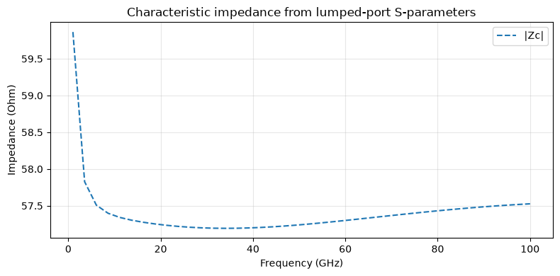
# Characteristic impedance from lumped-port S-parameters
import matplotlib.pyplot as plt
import numpy as np

z_ref = 50.0  # Palace reference impedance (Ohm)
freq_ghz = results.freq

s11 = results.s11.complex

try:
    # Preferred: full 2-port conversion S -> ABCD -> Zc
    s21 = results.s21.complex
    s12 = results.s12.complex
    s22 = results.s22.complex

    eps = 1e-15
    s21_safe = np.where(np.abs(s21) < eps, np.nan + 1j * np.nan, s21)

    A = ((1 + s11) * (1 - s22) + s12 * s21) / (2 * s21_safe)
    B = z_ref * ((1 + s11) * (1 + s22) - s12 * s21) / (2 * s21_safe)
    C = ((1 - s11) * (1 - s22) - s12 * s21) / (2 * z_ref * s21_safe)

    z_char = np.sqrt(B / C)
    # Branch choice: prefer positive real part
    z_char = np.where(np.real(z_char) < 0, -z_char, z_char)

    method = "2-port ABCD"
except Exception:
    # Fallback: input impedance from S11 (only exact for matched/load assumptions)
    z_char = z_ref * (1 + s11) / (1 - s11)
    method = "S11 input-impedance fallback"

print(f"Method: {method}")
print(f"Median Re(Zc): {np.nanmedian(np.real(z_char)):.2f} Ohm")
print(f"Median |Zc|: {np.nanmedian(np.abs(z_char)):.2f} Ohm")

fig, ax = plt.subplots(1, 1, figsize=(8, 4))
ax.plot(freq_ghz, np.abs(z_char), "--", label="|Zc|")
ax.set_xlabel("Frequency (GHz)")
ax.set_ylabel("Impedance (Ohm)")
ax.set_title("Characteristic impedance from lumped-port S-parameters")
ax.grid(True, alpha=0.3)
ax.legend()
plt.tight_layout()
plt.show()
Method: 2-port ABCD
Median Re(Zc): 57.31 Ohm
Median |Zc|: 57.32 Ohm
from pathlib import Path

import matplotlib.pyplot as plt
import numpy as np
import pyvista as pv

from gsim.palace import load_fields

pv.OFF_SCREEN = True

# Get results dir from sim output (or hardcode for re-runs)
results_dir = Path(results.files["port-S.csv"]).parent
# results_dir = Path("./sim-palace-mzm/")
print(f"Results dir: {results_dir}")

vol = load_fields(results_dir, excitation=1)
bnd = load_fields(results_dir, excitation=1, boundary=True)

print(f"Volume: {vol.n_points:,} points, {vol.n_cells:,} cells")
print(f"Boundary: {bnd.n_points:,} points, {bnd.n_cells:,} cells")

# Read physical groups from palace.msh
import meshio

mesh_candidates = [
    results_dir.parent / "input" / "palace.msh",
    results_dir.parent.parent / "palace.msh",
    results_dir / "palace.msh",
]
msh_path = next((p for p in mesh_candidates if p.exists()), None)
if msh_path is None:
    raise FileNotFoundError(
        f"Could not find palace.msh. Tried: {[str(p) for p in mesh_candidates]}"
    )

mio = meshio.read(msh_path)

# 1) Find boundary attribute IDs corresponding to physical_group 'metal3_xy'
metal3_attr = [
    int(tag)
    for name, (tag, dim) in mio.field_data.items()
    if "metal3_xy" in name.lower() and int(dim) == 2
]
if not metal3_attr:
    raise ValueError(
        f"Could not find 2D physical group 'metal3_xy' in {msh_path}. "
        f"Available groups: {sorted(mio.field_data.keys())}"
    )
print(f"metal3_xy boundary attribute IDs: {metal3_attr}")

# 2) Find which cell-data array in boundary mesh stores physical IDs
candidate_attr_names = ["attribute", "gmsh:physical", "PhysicalIds", "PhysicalId"]
attr_name = next((name for name in candidate_attr_names if name in bnd.cell_data), None)
if attr_name is None:
    raise KeyError(
        f"No boundary attribute array found. Available cell_data keys: {list(bnd.cell_data.keys())}"
    )

attrs = np.asarray(bnd.cell_data[attr_name]).astype(int)
mask = np.isin(attrs, metal3_attr)
cell_ids = np.flatnonzero(mask)
if cell_ids.size == 0:
    raise ValueError(
        f"No boundary cells matched metal3_xy IDs {metal3_attr} in array '{attr_name}'."
    )

# 3) Extract only the metal3 surface
metal_surface = bnd.extract_cells(cell_ids)
print(
    f"Extracted metal surface: {metal_surface.n_points:,} points, {metal_surface.n_cells:,} cells"
)

# 4) FEM-consistent interpolation from tetrahedra (VTK probe via sample)
need_point_conversion = (
    "E_real" in vol.cell_data and "E_real" not in vol.point_data
) or ("E_imag" in vol.cell_data and "E_imag" not in vol.point_data)
vol_for_sampling = (
    vol.cell_data_to_point_data(pass_cell_data=True) if need_point_conversion else vol
)
print(
    "Converted source cell data to point data for tetrahedral interpolation."
) if need_point_conversion else print(
    "Using source point data for tetrahedral interpolation."
)

metal_surface_fields = metal_surface.sample(vol_for_sampling, tolerance=1e-6)
print("Sampled arrays:", sorted(metal_surface_fields.array_names))

valid_key = "vtkValidPointMask"
if valid_key in metal_surface_fields.array_names:
    valid_mask = np.asarray(metal_surface_fields[valid_key]).astype(bool)
    valid_fraction = float(np.mean(valid_mask))
    print(f"Valid probe-point fraction: {valid_fraction:.3f}")
else:
    valid_mask = np.ones(metal_surface_fields.n_points, dtype=bool)
    print("No vtkValidPointMask found; assuming all sampled points are valid.")

# 5) Build |E| = sqrt(|E_real|^2 + |E_imag|^2)
if (
    "E_real" not in metal_surface_fields.array_names
    or "E_imag" not in metal_surface_fields.array_names
):
    raise KeyError(
        f"Expected E_real and E_imag in sampled arrays. Found: {sorted(metal_surface_fields.array_names)}"
    )

e_real = np.asarray(metal_surface_fields["E_real"])
e_imag = np.asarray(metal_surface_fields["E_imag"])

if e_real.ndim == 1:
    e_abs = np.sqrt(e_real**2 + e_imag**2)
else:
    e_abs = np.sqrt(np.sum(e_real**2 + e_imag**2, axis=1))

# Mark invalid probe points as NaN so they are not interpreted as physical zeros
e_abs = np.where(valid_mask, e_abs, np.nan)
metal_surface_fields["E_abs"] = e_abs
print(
    f"|E| stats (valid points): min={np.nanmin(e_abs):.3e}, max={np.nanmax(e_abs):.3e}"
)

# Top conductor z for convenience in slice-based comparisons
z_conductor = float(np.max(metal_surface.points[:, 2]))
print(f"z_conductor (from metal3_xy surface): {z_conductor:.3f} um")

# Plot |E| on the extracted metal3_xy surface
p = pv.Plotter(notebook=True)
p.add_mesh(
    metal_surface_fields,
    scalars="E_abs",
    cmap="turbo",
    opacity=1.0,
    show_edges=False,
    nan_color="black",
    scalar_bar_args={"title": "|E| (V/m)"},
)
p.add_text("|E| on metal3_xy (tetrahedral interpolation)", font_size=10)
p.show(jupyter_backend="static")
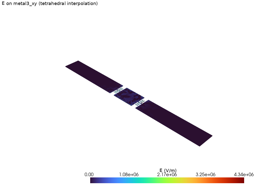
Results dir: sim-data-palace-9096ed0a/output


Volume: 3,696,860 points, 369,686 cells
Boundary: 929,736 points, 154,956 cells


metal3_xy boundary attribute IDs: [3]
Extracted metal surface: 409,848 points, 68,308 cells
Using source point data for tetrahedral interpolation.


Sampled arrays: ['B_imag', 'B_real', 'E_imag', 'E_real', 'J_s_imag', 'J_s_real', 'Q_s_imag', 'Q_s_real', 'S', 'U_e', 'U_m', 'attribute', 'attribute', 'vtkGhostType', 'vtkGhostType', 'vtkOriginalCellIds', 'vtkOriginalPointIds', 'vtkValidPointMask']
Valid probe-point fraction: 1.000
|E| stats (valid points): min=0.000e+00, max=4.338e+06
z_conductor (from metal3_xy surface): 5.200 um
from gsim.palace import EigenmodeSim

# Floquet eigenmode simulation (periodic in x)
sim = EigenmodeSim()
sim.set_output_dir("./palace-sim-mzm-floquet")
sim.set_geometry(mzm_cpw_comp)
sim.set_stack()
sim.set_airbox(margin_x=0, margin_y=20.0, z_above=100, z_below=100)
sim.set_eigenmode(
    num_modes=5,
    target=50e9,
    floquet=True,
    phi_target=1.5708,
    n_eff_guess=2.2,
)

sim.mesh(preset="fine", periodic_axis="x", max_mesh_size=15.0, refined_mesh_size=2.5)
sim.write_config()

# Static rendering keeps the mesh visible in the published Markdown.
sim.plot_mesh(
    show_groups=[
        "metal3_xy",
        "metal3_z",
        "P1_E0",
        "P1_E1",
        "P2_E0",
        "P2_E1",
        "SiO2",
        "passive",
    ],
    transparent_groups=["air__passive", "SiO2__passive"],
    style="solid",
    interactive=False,
)
Info : Reading 'palace-sim-mzm-floquet/palace.msh'...
Info : 14785 nodes
Info : 96187 elements
Info : Storing section $Periodic as model attribute
Info : Done reading 'palace-sim-mzm-floquet/palace.msh'
Info : Reading 'palace-sim-mzm-floquet/palace.msh'...
Info : 14785 nodes
Info : 96187 elements
Info : Storing section $Periodic as model attribute
Info : Done reading 'palace-sim-mzm-floquet/palace.msh'
Info : Reading 'palace-sim-mzm-floquet/palace.msh'...
Info : 14785 nodes
Info : 96187 elements
Info : Storing section $Periodic as model attribute
Info : Done reading 'palace-sim-mzm-floquet/palace.msh'
Info : Reading 'palace-sim-mzm-floquet/palace.msh'...
Info : 14785 nodes
Info : 96187 elements
Info : Storing section $Periodic as model attribute
Info : Done reading 'palace-sim-mzm-floquet/palace.msh'
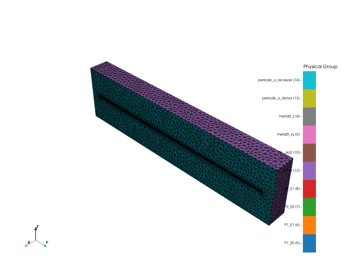
[34m18:13:21[0m | [33m[22mWARNING [0m | [33m[22mpyvirtualdisplay not available; continuing without Xvfb[0m