Running Palace Simulations
Palace is an open-source 3D electromagnetic simulator supporting eigenmode, driven (S-parameter), and electrostatic simulations. This notebook demonstrates using the gsim.palace API to run a driven simulation on a CPW (coplanar waveguide) structure.
Requirements:
- IHP PDK:
uv pip install ihp-gdsfactory - GDSFactory+ account for cloud simulation
Load a pcell from IHP PDK
import gdsfactory as gf
from ihp import LAYER, PDK

PDK.activate()

# IHP SG13G2 via design rules
_VIA_RULES = {
    "TopVia2": {
        "size": 0.9,
        "spacing": 1.06,
        "enclosure": 0.5,
        "layer": LAYER.TopVia2drawing,
    },
    "TopVia1": {
        "size": 0.42,
        "spacing": 0.42,
        "enclosure": 0.42,
        "layer": LAYER.TopVia1drawing,
    },
}


@gf.cell
def _via_block(
    cols: int = 2,
    rows: int = 2,
    via_type: str = "TopVia2",
) -> gf.Component:
    """Create a block of vias following IHP design rules."""
    c = gf.Component()
    rules = _VIA_RULES[via_type]
    size = rules["size"]
    pitch = size + rules["spacing"]  # center-to-center

    via = gf.c.rectangle((size, size), layer=rules["layer"])
    for col in range(cols):
        for row in range(rows):
            ref = c << via
            ref.move((col * pitch, row * pitch))

    return c


def _via_pad_width(cols: int, via_type: str) -> float:
    """Width of via pad (via array + enclosure on both sides)."""
    rules = _VIA_RULES[via_type]
    pitch = rules["size"] + rules["spacing"]
    return (cols - 1) * pitch + rules["size"] + 2 * rules["enclosure"]


def _place_via_block(c, via_block, x, y_ctr, via_type, cols, rows):
    """Place a via block centered vertically at y_ctr."""
    rules = _VIA_RULES[via_type]
    pitch = rules["size"] + rules["spacing"]
    vb = c << via_block
    vb.move((x + rules["enclosure"], y_ctr - ((rows - 1) * pitch + rules["size"]) / 2))


@gf.cell
def gsg_electrode_tm2_tm1_m5(
    tm2_length: float = 100,
    tm1_length: float = 50,
    m5_length: float = 300,
    s_width: float = 20,
    g_width: float = 40,
    gap_width: float = 15,
    tv2_cols: int = 2,
    tv2_rows: int = 10,
    tv1_cols: int = 4,
    tv1_rows: int = 10,
) -> gf.Component:
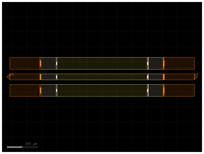
    """GSG electrode: TM2 -> TopVia2 -> TM1 -> TopVia1 -> M5 -> TopVia1 -> TM1 -> TopVia2 -> TM2.

    Args:
        tm2_length: Length of TM2 sections at each end (um)
        tm1_length: Length of TM1 sections between vias (um)
        m5_length: Length of Metal5 section in the middle (um)
        s_width: Signal trace width (um)
        g_width: Ground trace width (um)
        gap_width: Gap between signal and ground (um)
        tv2_cols/rows: TopVia2 array size
        tv1_cols/rows: TopVia1 array size
    """
    c = gf.Component()

    tv2_w = _via_pad_width(tv2_cols, "TopVia2")
    tv1_w = _via_pad_width(tv1_cols, "TopVia1")

    # Total length: TM2 | TV2 | TM1 | TV1 | M5 | TV1 | TM1 | TV2 | TM2
    total = 2 * tm2_length + 2 * tv2_w + 2 * tm1_length + 2 * tv1_w + m5_length

    # Section x-coordinates (left edges, centered at x=0)
    x = -total / 2
    sections = [
        ("tm2_l", tm2_length),
        ("tv2_l", tv2_w),
        ("tm1_l", tm1_length),
        ("tv1_l", tv1_w),
        ("m5", m5_length),
        ("tv1_r", tv1_w),
        ("tm1_r", tm1_length),
        ("tv2_r", tv2_w),
        ("tm2_r", tm2_length),
    ]
    xs = {}
    for name, width in sections:
        xs[name] = x
        x += width

    # Via blocks
    tv2_block = _via_block(cols=tv2_cols, rows=tv2_rows, via_type="TopVia2")
    tv1_block = _via_block(cols=tv1_cols, rows=tv1_rows, via_type="TopVia1")

    # GSG traces
    traces = [
        (0, s_width),
        (s_width / 2 + gap_width + g_width / 2, g_width),
        (-(s_width / 2 + gap_width + g_width / 2), g_width),
    ]

    TM2 = LAYER.TopMetal2drawing
    TM1 = LAYER.TopMetal1drawing
    M5 = LAYER.Metal5drawing

    for y_ctr, w in traces:
        yb = y_ctr - w / 2

        # TM2 left
        (c << gf.c.rectangle((tm2_length, w), layer=TM2)).move((xs["tm2_l"], yb))

        # TopVia2 left transition (TM2 + TM1 overlap + vias)
        (c << gf.c.rectangle((tv2_w, w), layer=TM2)).move((xs["tv2_l"], yb))
        (c << gf.c.rectangle((tv2_w, w), layer=TM1)).move((xs["tv2_l"], yb))
        _place_via_block(
            c, tv2_block, xs["tv2_l"], y_ctr, "TopVia2", tv2_cols, tv2_rows
        )

        # TM1 left
        (c << gf.c.rectangle((tm1_length, w), layer=TM1)).move((xs["tm1_l"], yb))

        # TopVia1 left transition (TM1 + M5 overlap + vias)
        (c << gf.c.rectangle((tv1_w, w), layer=TM1)).move((xs["tv1_l"], yb))
        (c << gf.c.rectangle((tv1_w, w), layer=M5)).move((xs["tv1_l"], yb))
        _place_via_block(
            c, tv1_block, xs["tv1_l"], y_ctr, "TopVia1", tv1_cols, tv1_rows
        )

        # Metal5 middle
        (c << gf.c.rectangle((m5_length, w), layer=M5)).move((xs["m5"], yb))

        # TopVia1 right transition
        (c << gf.c.rectangle((tv1_w, w), layer=TM1)).move((xs["tv1_r"], yb))
        (c << gf.c.rectangle((tv1_w, w), layer=M5)).move((xs["tv1_r"], yb))
        _place_via_block(
            c, tv1_block, xs["tv1_r"], y_ctr, "TopVia1", tv1_cols, tv1_rows
        )

        # TM1 right
        (c << gf.c.rectangle((tm1_length, w), layer=TM1)).move((xs["tm1_r"], yb))

        # TopVia2 right transition
        (c << gf.c.rectangle((tv2_w, w), layer=TM2)).move((xs["tv2_r"], yb))
        (c << gf.c.rectangle((tv2_w, w), layer=TM1)).move((xs["tv2_r"], yb))
        _place_via_block(
            c, tv2_block, xs["tv2_r"], y_ctr, "TopVia2", tv2_cols, tv2_rows
        )

        # TM2 right
        (c << gf.c.rectangle((tm2_length, w), layer=TM2)).move((xs["tm2_r"], yb))

    # Ports at TM2 ends
    c.add_port(
        name="o1",
        center=(-total / 2, 0),
        width=s_width,
        orientation=180,
        port_type="electrical",
        layer=TM2,
    )
    c.add_port(
        name="o2",
        center=(total / 2, 0),
        width=s_width,
        orientation=0,
        port_type="electrical",
        layer=TM2,
    )

    return c


c = gsg_electrode_tm2_tm1_m5()
cc = c.copy()
cc.draw_ports()
cc
Configure and run simulation with DrivenSim
from gsim.common.stack import get_stack
from gsim.palace import DrivenSim

# Create simulation object
sim = DrivenSim()

# Set output directory
sim.set_output_dir("./palace-sim-cpw")

# Set the component geometry
sim.set_geometry(c)

# Configure layer stack from active PDK
stack = get_stack(air_above=300.0)  # auto-detects active PDK
sim.set_stack(stack)

# Configure left CPW port (single port at signal center)
sim.add_cpw_port("o1", layer="topmetal2", s_width=20, gap_width=15)

# Configure right CPW port (single port at signal center)
sim.add_cpw_port("o2", layer="topmetal2", s_width=20, gap_width=15)

# Configure driven simulation (frequency sweep for S-parameters)
sim.set_driven(fmin=1e9, fmax=100e9, num_points=300)

# Validate configuration
print(sim.validate_config())
Validation: PASSED


/tmp/ipykernel_4180/3762363585.py:14: UserWarning: get_stack(air_above/air_below) is deprecated and ignored. Use simulation.set_airbox(margin_x=..., margin_y=..., z_above=..., z_below=...).
  stack = get_stack(air_above=300.0)  # auto-detects active PDK
# Generate mesh with planar conductors (presets: "coarse", "default", "fine")
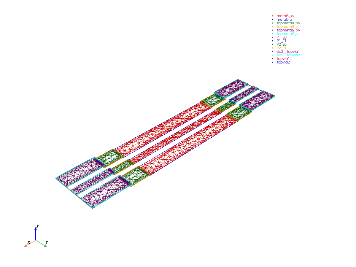
sim.mesh(preset="default", planar_conductors=False)
[34m22:33:28[0m | [33m[22mWARNING [0m | [33m[22mAbsorbing boundary is applied to solid dielectric surfaces (sin, sio2, topvia1, topvia2) because the model has no air region, which produces large spurious insertion loss and reflection. Add an airbox via set_airbox(margin_x=..., margin_y=..., z_above=..., z_below=...). Note that get_stack(air_above=...) is deprecated and ignored.[0m
Mesh Summary
========================================
Dimensions: 615.3 x 130.0 x 17.9 µm
Nodes: 7,196
Elements: 52,810
Tetrahedra: 34,866
Edge length: 0.42 - 26.95 µm
Quality: 0.500 (min: 0.007)
SICN: 0.547 (all valid)
----------------------------------------
Volumes (4):
- topvia1 [1]
- topvia2 [2]
- sio2 [3]
- sin [4]
Surfaces (15):
- metal5_xy [5]
- metal5_z [6]
- topmetal1_xy [7]
- topmetal1_z [8]
- topmetal2_xy [9]
- topmetal2_z [10]
- P1_E0 [11]
- P1_E1 [12]
- P2_E0 [13]
- P2_E1 [14]
- sio2__topvia1 [15]
- sio2__topvia2 [16]
- sio2__None [17]
- sin__sio2 [18]
- sin__None [19]
----------------------------------------
Mesh: palace-sim-cpw/palace.msh
Run simulation on cloud
  palace-a79961ce  completed  0m 00s


Extracting results.tar.gz...
Downloaded 12 files to /home/runner/work/simulation-templates/simulation-templates/docs/notebooks/sim-data-palace-a79961ce
Port mapping: Port 1: o1, Port 2: o2
Port mapping: Port 1: o1, Port 2: o2