Waveguide Crossing with Cosine Tapers
This notebook models a compact silicon waveguide crossing with cosine tapers using BeamZ. It demonstrates the geometry, simulation, and analysis workflow from end to end. It follows the Tidy3D Waveguide Crossing reference notebook.
To achieve high integration density on a photonic chip, efficient routing of light with compact, low-loss junctions is necessary. Waveguide crossings are therefore important building blocks in high-performance photonic integrated circuits.
The convex cosine taper focuses the guided mode at the crossing center so that most power is transmitted to the through port instead of scattering into the cross ports. The design is adapted from Sujith Chandran, et al. "Beam shaping for ultra-compact waveguide crossings on monolithic silicon photonics platform," Opt. Lett. 45, 6230-6233 (2020).
BeamZ is in beta
BeamZ is under active development. APIs, numerical behavior, and results may change between releases. Validate simulations independently before relying on them for design or production decisions.
Documentation note: The figures and text outputs embedded below are reference outputs bundled from the BeamZ v0.5.0 example notebooks (Apache-2.0). The code targets BeamZ v0.5.0; run the notebook to regenerate results for your local environment.
import os

import matplotlib.pyplot as plt
import numpy as np

try:
    from IPython.display import display
except ImportError:
    display = print
from scipy.optimize import fsolve
from shapely.geometry import Polygon as ShapelyPolygon
from shapely.geometry import box as shapely_box
from shapely.ops import unary_union

import beamz as bz

test_mode = os.environ.get("BEAMZ_DOCS_TEST") == "1"
um = bz.um  # unit scale in um

plt.rcParams.update({"figure.dpi": 120})
print(f"BeamZ version: {bz.__version__}")
BEAMZ version: 0.4.2
Simulation Setup
Define geometric parameters and materials. As in the reference design, the silicon waveguide has a thickness of 161 nm and an input width of 350 nm.
h = 0.161 * um  # waveguide thickness
w_in = 0.35 * um  # input taper width
w_out = 1.1 * um  # output taper width at the crossing center
w_m = 0.75 * um  # amplitude of the cosine function
l_t = 5.3 * um  # taper length
l_wg = 1.0 * um  # input/output straight waveguide length
n_si = 3.67
n_sio2 = 1.45

mat_si = bz.Material(permittivity=n_si**2)
mat_sio2 = bz.Material(permittivity=n_sio2**2)
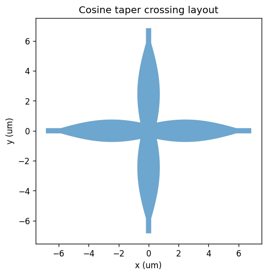
The taper width is described by a cosine function \(w(x)=w_m\cos(ax+b)\). We solve for \(a\) and \(b\) so that the taper starts at \(w_\mathrm{in}/2\) and reaches \(w_\mathrm{out}/2\) at the crossing junction. As in the reference notebook, one taper is generated first and the other three are made by symmetry. Before rasterization, the silicon pieces are merged into one polygon so shared boundaries do not create tiny grid seams.
# numerically solve for the cosine function that describes the taper shape
def equations(x0):
    a, b = x0
    return (
        w_m * np.cos(a * (-w_out / 2) + b) - w_out / 2,
        w_m * np.cos(a * (-w_out / 2 - l_t) + b) - w_in / 2,
    )


a, b = fsolve(equations, (0.5 / um, 2.0))

x = np.linspace(-w_out / 2 - l_t, -w_out / 2, 30)
w = w_m * np.cos(a * x + b)

# Construct one taper, then generate the remaining three by symmetry.
vertices_left = list(zip(np.r_[x, x[::-1]], np.r_[w, -w[::-1]]))
vertices_right = [(-xv, yv) for xv, yv in vertices_left]
vertices_top = [(yv, -xv) for xv, yv in vertices_left]
vertices_bottom = [(yv, xv) for xv, yv in vertices_left]
taper_vertex_sets = (vertices_left, vertices_right, vertices_top, vertices_bottom)


def _iter_polygons(geometry):
    if geometry.geom_type == "Polygon":
        return [geometry]
    if geometry.geom_type == "MultiPolygon":
        return list(geometry.geoms)
    raise ValueError(f"Expected Polygon or MultiPolygon, got {geometry.geom_type}")


def _ring_vertices(ring, z0=-h / 2):
    return [(float(xv), float(yv), z0) for xv, yv in list(ring.coords)[:-1]]


def silicon_union_2d(domain_size):
    lx, ly = domain_size
    pieces = [ShapelyPolygon(verts) for verts in taper_vertex_sets]
    pieces.extend(
        [
            shapely_box(-w_out / 2, -w_out / 2, w_out / 2, w_out / 2),
            shapely_box(-lx / 2, -w_in / 2, lx / 2, w_in / 2),
            shapely_box(-w_in / 2, -ly / 2, w_in / 2, ly / 2),
        ]
    )
    merged = unary_union(pieces)
    return merged if merged.is_valid else merged.buffer(0)


def merged_silicon_structures(domain_size, z0=-h / 2):
    return [
        bz.Polygon(
            vertices=_ring_vertices(polygon.exterior, z0),
            interiors=[_ring_vertices(ring, z0) for ring in polygon.interiors],
            material=mat_si,
            depth=h,
            z=z0,
        )
        for polygon in _iter_polygons(silicon_union_2d(domain_size))
    ]


fig, ax = plt.subplots(figsize=(5, 5))
for polygon in _iter_polygons(
    silicon_union_2d((2 * l_t + w_out + 2 * l_wg, 2 * l_t + w_out + 2 * l_wg))
):
    x_poly, y_poly = np.asarray(polygon.exterior.coords.xy) / um
    ax.fill(x_poly, y_poly, color="tab:blue", alpha=0.65, linewidth=0)
ax.set_aspect("equal")
ax.set_xlabel("x (um)")
ax.set_ylabel("y (um)")
ax.set_title("Cosine taper crossing layout")
plt.show()
BeamZ Rasterization Note
BeamZ rasterizes structures into a finite voxel/material grid before simulation. If overlapping or touching silicon objects are passed separately, each object can be anti-aliased independently. That can leave tiny numerical seams or asymmetries at shared boundaries, even when the analytical geometry describes the intended symmetric shape.
This notebook keeps the physical design from the reference, but adds three BeamZ-specific safeguards before rasterization:
- Use exact symmetric taper transforms: build the left taper once, then generate the right, top, and bottom tapers from that same reference shape.
- Merge silicon before rasterization: union the tapers, center square, and straight waveguides into one silicon polygon so BeamZ rasterizes one continuous region rather than several touching regions.
- Snap the domain to the grid: make the simulation domain an integer number of grid cells so the origin and mirror axes land symmetrically on the raster grid.
These steps do not change the physical design. They make the discrete BeamZ material grid preserve the symmetry of the analytical design.
Set up the simulation domain, source plane, and monitors. The source and flux planes use the original straight-section placement from the reference setup. The workflow is still: create an empty simulation, solve and inspect the local mode, then attach the mode source. The immutable ModeSource config owns the solve request, and BeamZ's native mode package handles solving and launch planning during preview and compilation.
lambda0 = 1.31 * um
freq0 = bz.LIGHT_SPEED / lambda0
ldas = np.linspace(1.26, 1.36, 5 if test_mode else 101)
lambdas = ldas * um
freqs = bz.LIGHT_SPEED / lambdas

fwidth = freq0 / 10
run_time = 6 / freq0 if test_mode else 1e-12

min_steps_per_wvl = 4 if test_mode else 10
dx = lambda0 / (min_steps_per_wvl * n_si)
grid_spec = bz.GridSpec.uniform(dx)


def snap_domain_to_grid(length, resolution):
    cells = int(np.ceil(length / resolution))
    # Nudge upward by one floating-point step so BeamZ int(length / dx)
    # cannot truncate to cells - 1 because of roundoff.
    return np.nextafter(cells * resolution, np.inf), cells


Lxy_target = 2 * l_t + w_out + 2 * l_wg
Lx, nx = snap_domain_to_grid(Lxy_target, dx)
Ly, ny = snap_domain_to_grid(Lxy_target, dx)
Lz, nz = snap_domain_to_grid(1.5 * lambda0, dx)
sim_size = (Lx, Ly, Lz)

pml_layers = 4 if test_mode else 12
pml_t = pml_layers * lambda0 / (min_steps_per_wvl * n_si)
source_x = -Lx / 2 + l_wg / 2
through_x = Lx / 2 - l_wg / 2
cross_y = Ly / 2 - l_wg / 2

# Merge the center square, four tapers, and straight waveguides into one silicon
# polygon set before rasterization. Rasterizing one merged object avoids tiny
# anti-aliased seams where separate equal-material objects overlap or touch.
structures = merged_silicon_structures((Lx, Ly), z0=-h / 2)

source_time = bz.GaussianPulse(
    freq0=freq0,
    fwidth=fwidth,
    offset=0.5 if test_mode else 4.0,
)
mode_spec = bz.ModeSpec(num_modes=1, target_neff=3.455, polarization="te")
boundaries = (
    bz.PML(
        thickness=pml_t,
        formulation="cpml",
        m=3,
        kappa_max=3.0,
        alpha_max=0.0,
    ),
)

plane_z_span = 4 * h
source_plane = bz.Box(center=(source_x, 0, 0), size=(0, 4 * w_in, plane_z_span))

field_monitor = bz.FieldMonitor(
    center=(0.0, 0.0, 0.0),
    size=(Lx, Ly, 0.0),
    freqs=[freq0],
    fields=("Ex", "Ey", "Ez"),
    name="field",
)

flux_monitor_through = bz.FluxMonitor(
    center=(through_x, 0, 0),
    size=(0, 4 * w_in, plane_z_span),
    freqs=freqs,
    name="flux_through",
)

flux_monitor_cross = bz.FluxMonitor(
    center=(0, cross_y, 0),
    size=(4 * w_in, 0, plane_z_span),
    freqs=freqs,
    name="flux_cross",
)

design = bz.Design(background=mat_sio2)
for structure in structures:
    design += structure

sim0 = bz.Simulation(
    domain=sim_size,
    grid_spec=grid_spec,
    design=design,
    sources=[],
    monitors=[field_monitor, flux_monitor_through, flux_monitor_cross],
    boundaries=boundaries,
    run_time=run_time,
)

print(f"dx = {sim0.resolution / um:.4f} um")
grid_shape = sim0.to_request(num_steps=1).materials.shape
print(f"grid = {grid_shape}, steps = {sim0.num_steps}")
print(
    f"target Lx/Ly = {Lxy_target / um:.4f} um; snapped Lx/Ly = {Lx / um:.4f} um ({nx} cells)"
)
print(f"snapped Lz = {Lz / um:.4f} um ({nz} cells)")
print(f"source/monitor x/y clearance to domain edge = {l_wg / (2 * um):.2f} um")
print(f"CPML width = {pml_t / um:.3f} um ({pml_layers} cells at the reference grid)")
print(f"source/monitor clearance to x/y CPML = {(l_wg / 2 - pml_t) / um:.2f} um")
print(
    f"source/monitor clearance to z CPML = {(Lz / 2 - pml_t - plane_z_span / 2) / um:.2f} um"
)
● Done: Raster cache hit (3d): 4ab95b24bed2dd13001c46cf46f58881947380e7944a4b18a911160c4e442be2.npz | load=0.19s
dx = 0.0357 um
grid = (56, 384, 384), steps = 14695
target Lx/Ly = 13.7000 um; snapped Lx/Ly = 13.7068 um (384 cells)
snapped Lz = 1.9989 um (56 cells)
source/monitor x/y clearance to domain edge = 0.50 um
CPML width = 0.428 um (12 cells at the reference grid)
source/monitor clearance to z CPML = 0.25 um
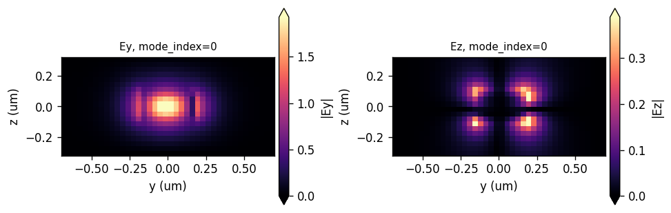
Solve the input waveguide modes on the source plane and convert the lowest-order TE-like mode into a BeamZ mode source.
mode_source_request = bz.ModeSource(
    center=source_plane.center,
    size=source_plane.size,
    direction="+",
    source_time=source_time,
    mode_spec=mode_spec,
    power=1.0,
)
modes = mode_source_request.solve_modes(sim0, freqs=[freq0])
assert np.all(np.isfinite(np.asarray(modes.neffs)))

from beamz.analysis import mode_data_to_dataframe
from beamz.analysis.plotting import plot_mode_field_components

fig, axes, neffs = plot_mode_field_components(
    modes,
    field_names=("Ey", "Ez"),
    mode_indices=(0,),
    val="abs",
    f=freq0,
    figsize=(8, 3),
    show=False,
)
display(mode_data_to_dataframe(modes))
plt.show()

# Attach the same immutable ModeSource config after inspection. Compilation will
# lower it into a native launch plan without mutating this object.
mode_source = mode_source_request
sim = sim0.updated_copy(sources=(mode_source,))
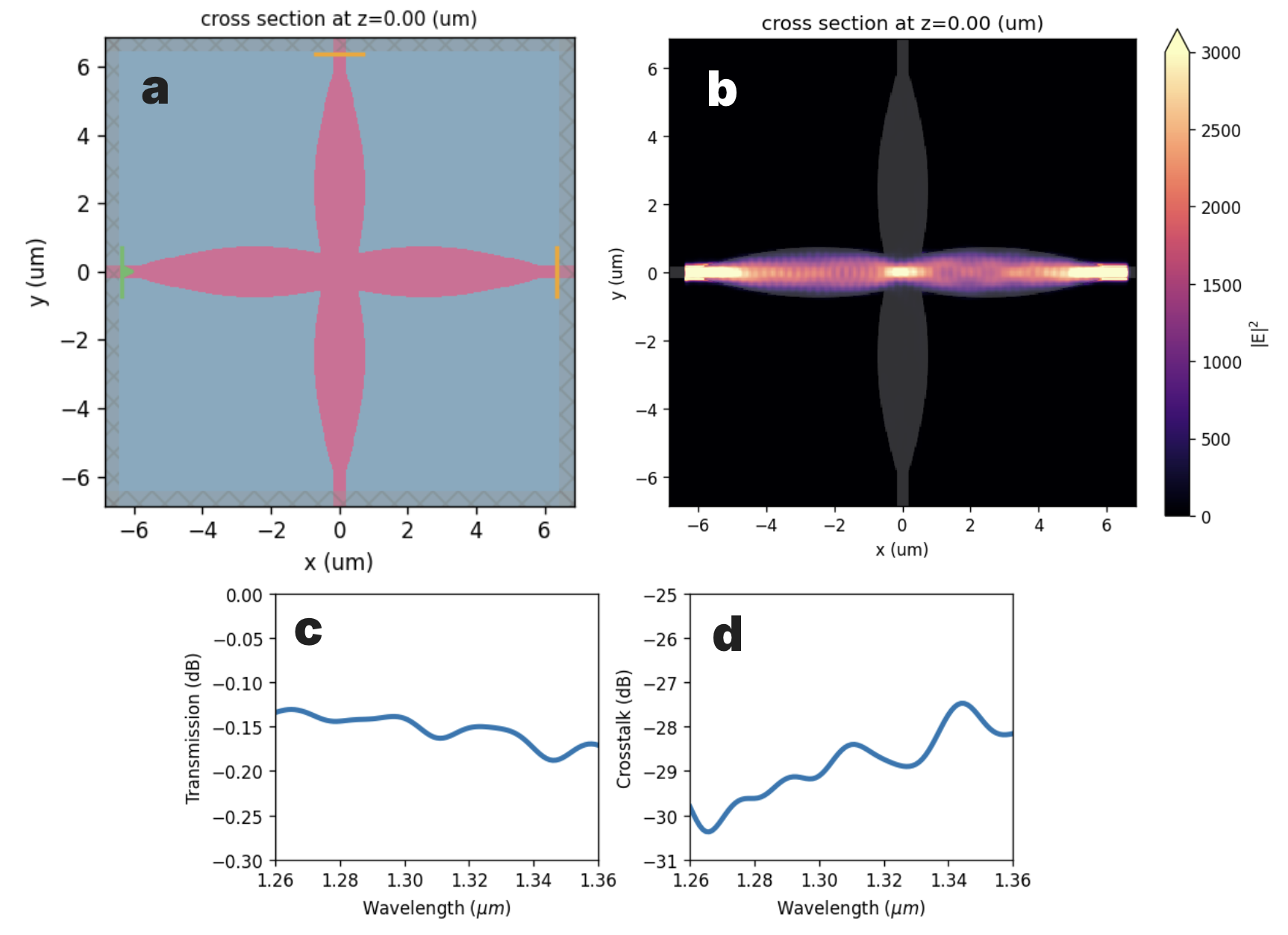
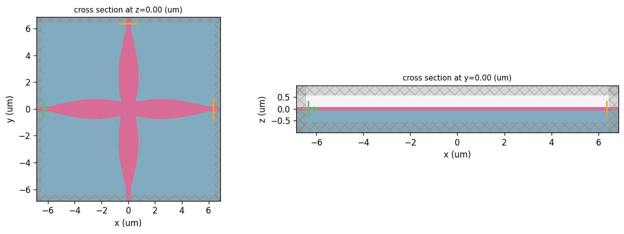
Before running the simulation, plot the structure, source, and monitor planes to verify the setup. BeamZ does not need a cloud job submission step; the simulation runs locally.
Run the crossing at the practical 10-steps-per-wavelength grid. ModeSource calibrates its emitted power as part of launch compilation, and the detached flux results apply the source waveform normalization automatically. No reference or input monitor is required.
● JIT compiling v0.3 packed FDTD program... done!
● Progress: 100% (14695/14695 steps)
Result Visualization
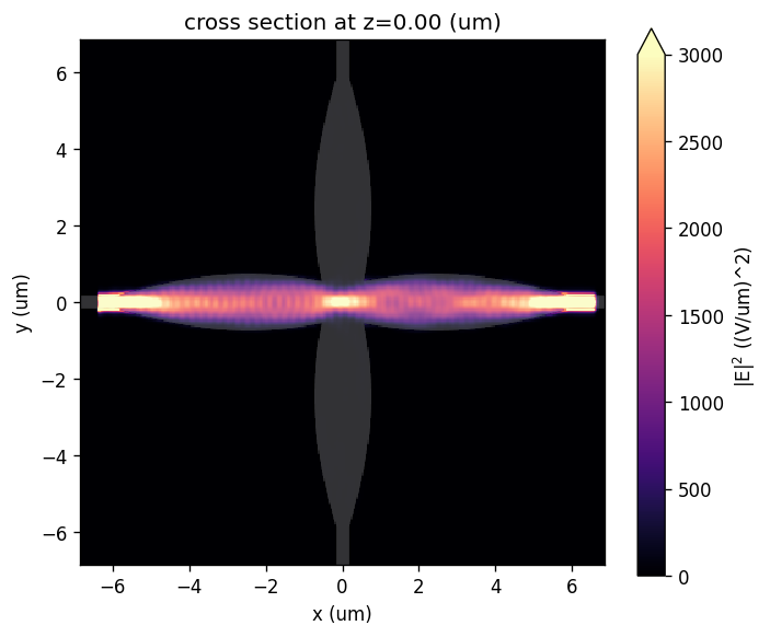
After the simulation completes, first plot the field distribution at the crossing plane. A strong field focus near the junction indicates that the cosine taper is shaping the mode before it reaches the crossing center.
sim_data.plot_field(
    field_monitor_name="field",
    field_name="E",
    val="abs^2",
    f=freq0,
    vmin=0,
    vmax=3000,
    cmap="magma",
    figsize=(6, 5),
)
plt.show()
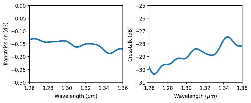
Finally, quantify the crossing performance over the O-band wavelength range. FluxMonitor.flux already includes the source waveform normalization and is reported in watts. The transmission denominator is SimulationResults.launched_power(): the solved source mode integrated with the mode solver's exact component-staggered transverse metric. The mode-source compiler uses that value to calibrate the launch to the requested 1 W, without adding an input monitor or reference simulation. Crosstalk is the cross-port power relative to through-port power. We plot 10 log10(T), which is negative for a passive device; positive insertion loss would instead use -10 log10(T).
f, (ax1, ax2) = plt.subplots(1, 2, tight_layout=True, figsize=(7, 3))

flux_through = sim_data["flux_through"].flux
flux_cross = sim_data["flux_cross"].flux
source_power = sim_data.launched_power(source=0)


def safe_power_ratio(numerator, denominator, floor=1e-30):
    numerator = np.asarray(numerator, dtype=float)
    denominator = np.asarray(denominator, dtype=float)
    ratio = np.zeros(
        np.broadcast_shapes(numerator.shape, denominator.shape), dtype=float
    )
    return np.divide(
        numerator, denominator, out=ratio, where=np.abs(denominator) >= floor
    )


T_through = safe_power_ratio(flux_through, source_power)
T_cross = safe_power_ratio(flux_cross, source_power)
assert np.all(np.isfinite(T_through))
assert np.all(np.isfinite(T_cross))
assert np.any(source_power > 0.0)

transmission_db = 10 * np.log10(np.maximum(T_through, 1e-30))
crosstalk_db = 10 * np.log10(np.maximum(safe_power_ratio(T_cross, T_through), 1e-30))
# print("Internally calibrated launched power (W):", source_power)
# print("Source-power-normalized transmission range (dB):",
#      float(transmission_db.min()), float(transmission_db.max()))

ax1.plot(ldas, transmission_db, lw=3)
ax1.set_xlabel(r"Wavelength ($\mu m$)")
ax1.set_ylabel("Transmission (dB)")
ax1.set_xlim((1.26, 1.36))
ax1.set_ylim((-0.3, -0))

ax2.plot(ldas, crosstalk_db, lw=3)
ax2.set_xlabel(r"Wavelength ($\mu m$)")
ax2.set_ylabel("Crosstalk (dB)")
ax2.set_xlim((1.26, 1.36))
ax2.set_ylim((-31, -25))
plt.show()