Ring coupler with GDSFactory FDTD
Run a 3D simulation using gsim.fdtd, a 60 nm Yee grid, and the active PDK. Exciting o1 returns one column of the S-matrix.
Requirements: gsim>=0.9.0 and GDSFactory+ cloud simulation access. To update an older project environment, run uv add "gsim>=0.9.0" "pdk-schema[sympy]~=0.3.0" from your project folder, then restart the notebook kernel.
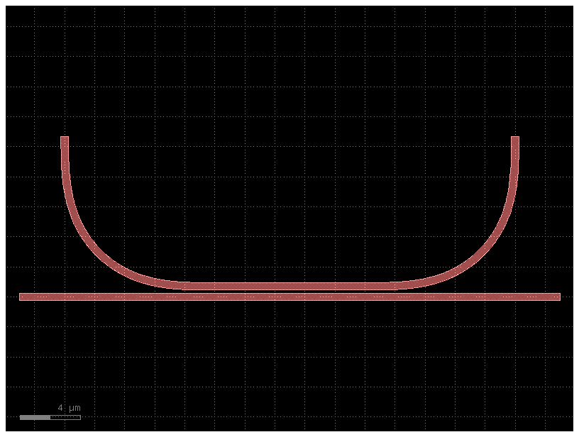
Load a component from the active PDK
import gdsfactory as gf

component = gf.get_component("coupler_ring", length_x=10)
component = component.copy()
component.auto_rename_ports()
component
Configure the 3D simulation
Use the PDK layer stack with lossless silicon (n = 3.47) and silica (n = 1.44) at 1.55 µm. Sweep 1.50–1.60 µm; weak source-spectrum tails are hidden in the plots.
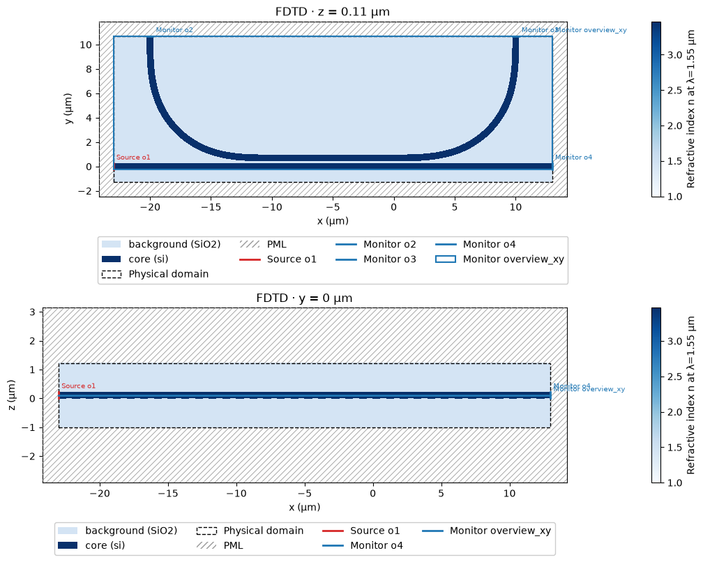
The curved-arm ports lie on the upper Y boundary. Add cladding below the bus with padding_y=(1.0, 0.0) so its sloped sidewalls fit inside the physical domain while the upper ports remain on the boundary.
from gsim import fdtd

sim = fdtd.Simulation(pdk=pdk)
sim.materials(background="SiO2", overrides={"si": 3.47, "SiO2": 1.44})
sim.geometry(component=component, geometry_tolerance_nm=10)
sim.source(
    port="o1",
    wavelength_um=1.55,
    wavelength_span_um=0.1,
    num_wavelengths=101,
)
sim.domain(padding=1.0, padding_y=(1.0, 0.0), pml_cells=20)
sim.solver(cell_size_nm=60, energy_decay_fraction=1e-6, max_wall_seconds=3600)
Inspect the geometry and record the field
The interactive 3D view shows the device geometry and ports. An XY monitor through the input waveguide core records field intensity at the center wavelength, separately from the guided-port S-parameter monitors.
core_z_um = sim.resolved.ports[sim.source.port].center[2]
sim.monitors.add_plane(
    name="overview_xy",
    center_um=(component.dx, component.dy, core_z_um),
    size_um=(component.dxsize, component.dysize, 0),
    normal="+z",
    flux=False,
    heatmap=fdtd.Heatmap(quantity="intensity", wavelengths_um=[1.55]),
)

sim.plot_3d()
Inspect 2D cross-sections
Static slices show the refractive index, the PML (hatched), the source, and the monitors the slice cuts. The XY slice passes through the waveguide core; the XZ slice runs along the input waveguide.
import matplotlib.pyplot as plt

port_y_um = sim.resolved.ports[sim.source.port].center[1]
fig, (ax_xy, ax_xz) = plt.subplots(2, 1, figsize=(10, 8), constrained_layout=True)
sim.plot_2d_static(axis="z", position_um=core_z_um, ax=ax_xy)
sim.plot_2d_static(axis="y", position_um=port_y_um, ax=ax_xz, aspect="auto")
plt.show()
Run on the cloud
Reuse a completed run when the simulation inputs match.
fdtd-7c87fd74  [####################]  Job completed  elapsed 0m 00s
Extracting results.tar.gz...
Downloaded 3 files to /home/runner/work/simulation-templates/simulation-templates/docs/notebooks/sim-data-fdtd-7c87fd74
Inspect the S-parameters
Inspect the split between the bus and curved coupling arm. This is an open four-port coupler, not a closed ring resonator.
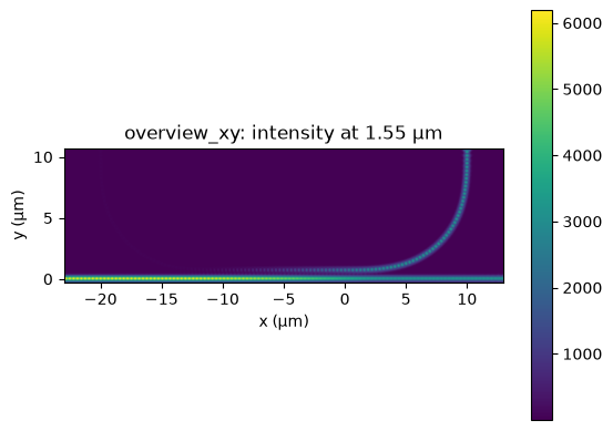
Field intensity
Use equal X and Y scales so a micrometer has the same displayed length in each direction.
field_figure, field_axis = result.monitors["overview_xy"].plot_heatmap(
    wavelength_um=sim.source.wavelength_um
)
field_axis.set_aspect("equal", adjustable="box")